6-13-08, This page is in
progress.
Much to be added.
11-22-08, Updated with more good poop. 11-29-11,
Added more good poop on how to fence a module.
I offer this page as a general
guide for the builders of the SLIM MSA. It is relevant for
building any circuit, not just the SLIMs. I will add items to
this page as time goes on.
Topics
Covered on this Page
Prevent Trouble
Static Electricity Precautions
Wiring Interconnections
RF Connector Installations
Direct Coaxial Cable Connections
Fencing and shielding
Component soldering
Component Cleaning
Component removal
Measuring Power and Voltage
Nice to know Links:
Types of RF
Connectors with pictures. Prevent Trouble
When a proven design is built, there are only two
reasons why it won't work.
One or more components are bad from the manufacturer. Very
unlikely! Or, the builder screwed it up. Highly
likely!
To prevent this, I will discuss a few things that will save you much
grief.
Here are the most common construction errors and how to avoid them.
1. Bad solder connections
Almost all of the parts used in the SLIMs are
surface mounted devices, SMD's. When they come off the assembly
line, they are perfect and ready to be used. However, they can
sit on a shelf for a long period of time before you use them.
Their solder connections can become corroded, or tarnished, and will
reject a good
solder flow. Use a good magnifying glass when installing
components. Look closely at their solder connection points.
If there is any doubt as to their cleanliness, use some type of
burnisher to clean them until they shine. I like to
use a pencil erasure. Do not use any chemical that may
leave a residue. I like at least 90 per cent isopropyl
alcohol. And for goodness sakes, DO NOT blow on an alcohol-wet
part to dry it. It will absorb the moisture in your breath and
leave water marks. This includes circuit boards. Check out your
local pharmacy. I found 99% isopropyl at Safeway, and Tom Thumb
supermarkets.
2. Wrong part in wrong position
A good carpenter will tell you, "measure
twice and cut once". I suggest you make doubly sure you are
installing the correct part. Make sure the polarity is
correct. And certainly, make sure the component is installed on
to the correct pads. The SLIM's pwbs do not have a silkscreen
layer with markings for components. However, each SLIM has a
document called LAYSLIM-xx-yy. It is the only document
to be used for placing parts in the correct position.
Make absolutely sure the part is the correct
part. Almost all chip capacitors and inductors look alike.
Unless you trust your parts vendor (I don't), measure these parts with
your trusty AADE L/C meter.
3.
Destroyed
parts
SMD's are not only small, but usually
quite brittle. Do not use excessive force when installing or
removing these devices.
Also, electrostatic discharge (ESD) can
destroy a component without you knowing it. Install your
components in a good ESD environment. See paragraph relating to
Static Electricity Precautions.
4. Solder bridges
Too much solder is just as bad as not enough
solder. Usually, solder bridges between component pins are very
obvious. But, if signal traces are running under a component,
solder bridging can occur without them being seen. Once the
soldering process is completed, use a good magnifying glass or
microscope to inspect each and every solder joint. You cannot
inspect a joint too many times. Believe me, multiple inspection
is not a waste
of time.
Static Electricity Precautions
I won't beat this subject to death. I
will just give you a hint for a simple static
free work area. For a very easy and cheap working surface, use an
aluminum cookie sheet. It must be untreated and unpainted.
(not teflon). Fabricate a length of hook-up wire with alligator
clips on each end. Clip one to the cookie sheet, the other to the
ground of your test equipment or soldering iron base.
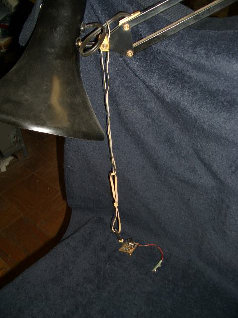
Wiring Interconnections
Power and Signal Interconnections between SLIMs are
multipin wiring. I standardized the multipin
connectors as .1 inch spaced, vertical pin headers. They can be
purchased in strips of 36 pins, and cut to the preferred length.
As an option, headers can be deleted, and point to point wires can be
directly soldered. For direct soldering to the header pins, the
Tin plated headers (that are called out in the parts lists) are
fine. If gold plated female mating connectors are preferred, then
substitute gold plated header pins for the modules. I do not
recommend using any mating connector that is not gold plated.
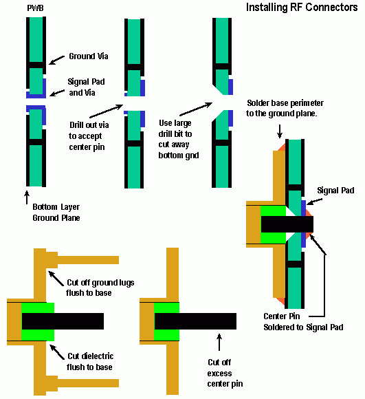
RF Connector Installations for
SLIMs
If an RF connector is installed, the center
hole must be
drilled out to the size of the center post of the RF connector.
This hole size varies among connectors, but .035 inch is common.
The bottom center pad is allowed to be destroyed, since the 0.080
pad on the top component layer will be soldered to the center
pin. On the bottom, if there
is little, or no, clearance from the center hole to ground, the
clearance
can be widened by grinding the ground area away, using a large (sharp)
drill bit. This makes a "V" shaped gouge around the center hole,
without widening the via hole on the top surface. If the RF
connector
has ground lugs, they must be cut off flush to the base, with a Dremel
type tool. The RF connector is then placed flush to the ground
plane and the base soldered around it's perimeter. This is
actually a better RF ground connection than with ground lugs and
mounting post
holes.
In this diagram, notice the comment "Cut dielectric flush to
base". When the connector is heated during the solder process,
the dielectric will swell and expand. This will cause the
connector to push itself away from the pwb. It is a good idea to
pretreat the connector before installing on the pwb. Do this by
heating the connector and allowing the dielectric to expand.
While it is still hot, use a sharp blade to cut the dielectric flush to
the base. When it cools, the dielectric will retract, leaving an
internal gap. Then, when the connector is soldered to the pwb,
the dielectric will expand again, but only to the plane of the
connector's base.
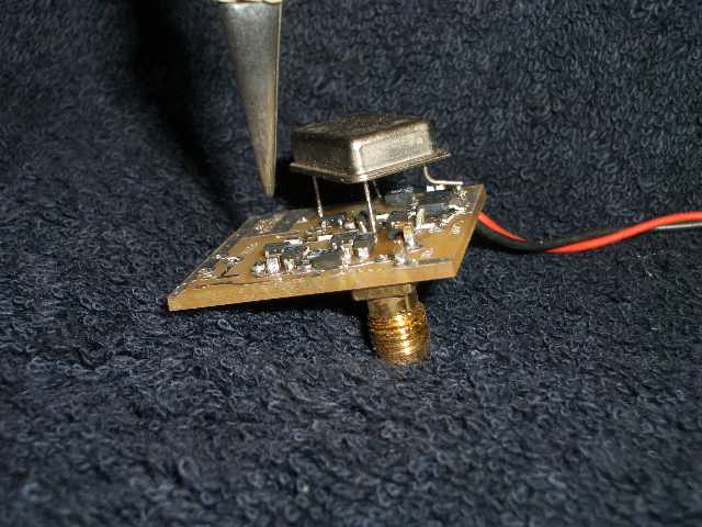
Direct
Coaxial Cable Connections
I have created a somewhat, unorthodox way of
coaxial cable interconnections. Normally, RF connectors are
mounted on
the bottom of the SLIM. However, due to limited real real estate,
many RF pcb connectors need to be modified. And, since RF pcb
connectors are a major expense, I have created a way to connect coax
directly to the board, while retaining excellent RF
characteristics.
Every SLIM module with an RF connection
has been
designed and layed out to accomodate a direct coaxial cable
connection. The top layer connection (signal pad) is a .08 inch
diameter round
pad, with a hole diameter of 0.020 inch. The bottom layer is a
.041 diameter round pad with the .020 hole. It is surrounded by a
ground ring that has an inside radius of .030 inch and an outside
radius of .090 inch. The ground ring is not noticed
since
it is connected to the bottom layer ground plane.
This allows a clearance of 0.010 inch
between the center pad and the ground ring. However, this is a
very narrow
clearance, and it is advisable to cut away the bottom center conductor
pad, using a sharp drill bit.
The coax cable is
connected on the bottom layer with its center conductor passing through
the 0.020 hole and its outer shield soldered to the ground ring.
Both RG-188 soft coax and RG-085 hard pipe have center conductor
diameters of 0.020 inch. Sometimes the pwb house will over-plate,
and the .020 holes will "shrink" to .019 or less. If this
happens, simply insert a steel pin (steal one from your wife) and
"wiggle" the hole a little larger.
When the cable is heated during the solder process, the
dielectric will swell and expand. This will cause the cable
to
push itself away from the pwb. It is a good idea to pretreat the
cable before installing to the pwb. Do
this by heating the cable and allowing the
dielectric to expand. While it is still
hot, use a sharp blade to cut the dielectric flush to the outer
shield. When
it cools, the dielectric will retract, leaving an internal gap.
Then, when the cable is soldered to the pwb, the
dielectric will expand again, but
only to the plane of the outer shield. Be sure to cut off the
excess center pin on the top side of the pwb. At high
frequencies, excess pin length acts like a tiny antenna.
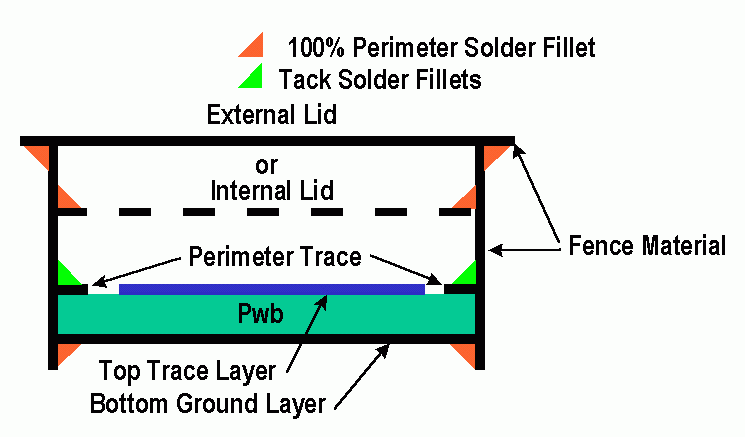
Fencing and Shielding
Most SLIM modules are
totally shielded to prevent RF interference. I use a
1/2 to 1 inch tall "fence" cut from a coffee can lid (tin plated
steel), placed
around the
perimeter of the module's pwb and soldered on both sides of the
board. A cover is formed from the same material, so that it fits
within
the top
of each module's fence. After testing is complete, the lids can
be
fully soldered to the fence. Copper or brass is optional.
The lid can be installed externally (on the top of the fences) or
internally (recessed within the module). Either is acceptable. Internal
lids are easier to install, but more difficult to remove.
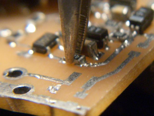
Component Soldering
Much has been written on soldering
techniques. Many builders prefer to mount SMD's using solder
paste and reflowing all connections at one time. Personally, I
still use the old fashon method. Ye olde soldering iron.
All components have two or more solder point connections. When
one point is connected to a ground pad, there is usually a via very
close, connected to the ground plane on the bottom of the pwb.
This pad really "sucks up" the heat of the soldering iron, and poor
solder joints can occur.
Here is how I do it, using a chip capacitor as an
example. Look at the receiving pads on the pwb, and determine
which pad is going to be the least difficult to accept a good solder
joint. Pretin this pad with your soldering iron using flux and
solder, or multicore flux solder. Do I need to say, 60/40
solder? For goodness sakes, DO NOT USE lead free solder.
Use it for fishing weights. Pretin the correct end of the
capacitor for this pad. Do not clean the flux from either the
pretinned capacitor or the pwb pad. There will be enough flux
remaining for the next step. Now, hold the capacitor on the
correct pads using your favorite tweezers. The capacitor will not
be flush to the board, due to the pretinning. Now, apply the
soldering iron tip to the pretinned areas of both the capacitor and
pad, and allow the solder to
flow. The capacitor will now sink flush to the pwb.
Repeat this process for all the components to be
mounted on the pwb. Some components will have multiple pads that
will very easily accept solder. Go ahead and solder these joints,
leaving the "heat sucking" pads for the next step. If a component
is fully soldered, take a black dry marker and mark the top of the
component, as if to say, "nothing else needs to be done to this
component".
Now, for the final soldering step. We are going to heat
the pwb to about 100 degrees C, or 212 degrees F, and solder the
remaining pads. For a heater, I use the base plate of my coffee
maker. It will actually get much hotter than needed so
precautions must be maintained. Place the coffee maker on the
static free work area. I turn it on and allow it to warm up, and
occasionally, touch the base plate with a wet finger. When the
finger moisture begins to sizzle, it is 100 degrees, C. Remove
power from the coffee maker. Set the pwb on the hot base
plate. Begin soldering the remaining "heat sucking" joints.
They will accept solder quite well. After about 1 minute, remove
the pwb from the base plate. Re-power the coffee maker and allow
it to build it's heat back to 100 degrees, C, using the wet finger
indication. Remove power, reposition the pwb, and continue the
solder process. Use this technique until all components are
soldered. The black marks on the previously completed components
will save you time by not searching for components that don't need
soldering.
When completed, wash and clean the board with
isopropyl alcohol (90 % or better). The black marks will wash
away with alcohol. Some black permanent markers will not clean
away. Test your marker to make sure it will clean up with
alcohol. If it doesn't, don't use the marker. Any residue
is conductive and will make your life miserable with unknown or "weird"
electrical problems later.
Component Cleaning
Here is the best method for cleaning.
Go to the hardware store, plumber's section and ask
for "acid brushes". Also called "flux brush". They are used to apply
flux to copper tubing before soldering. They are cheap, about 20 cents.
Get several. The bristles are about 1 inch long. Cut them back to 1/2
inch, making the brush stiffer. Also, go to your pharmacist and ask for
"pure" isopropyl. He may direct you to 99 or 100 %. I get my 99% at
Kroger (aka Safeway or Piggly Wiggly).
Lay out 3 small containers to hold the alcohol. I use the little
plastic containers that hold the icing in the cinnamon rolls. About a
teaspoon in the first. Just a few drops in the other two. Use 3 acid
brushes, one for each. This prevents cross contamination.
1. Use enough alcohol from the first to well saturate the components.
Drown them. Let the unit sit for a minute to let the flux soften. Then
scrub. Use a paper towel to absorb the "wash". Repeat twice.
2. Use brush 2 and container 2 and scrub again. Use clean area of paper
towel to blot up the "wash".
3. Use brush 3 and container 3 and scrub again. Use clean area of paper
towel to blot up the "wash".
Let the unit dry naturally. You can "fan" it, but do not blow on it.
After drying hold unit and look for "stains", "rings" around
components, etc. If you see anything, it is not clean. Visual
inspection under components is impossible, but if there is any flux
under them, the "rings" are a giveaway to leftover flux.
Component removal
Removing surface mounted devices (SMD's) from a
printed wiring board is an art. An improper removal technique can
result in destruction of the SMD, traces, pads, and even neighboring
components. I will give a few techniques that have proven well
over my many years of experience. I'll split the discussion into
two parts, dual lead SMD's and multi-lead SMD's.
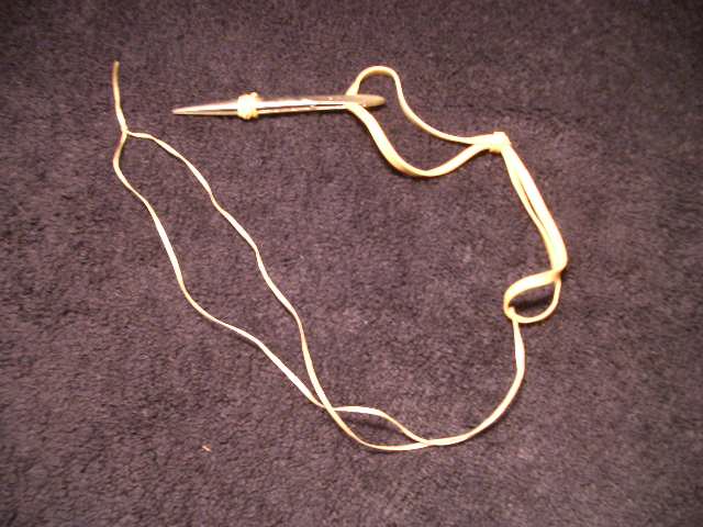
Dual lead SMD's are very easy to remove and I have
developed a technique that is a guaranteed winner. I call it the
"Third Hand Technique". What you will need: ESD workstation, two
soldering irons, sharp pointed tweezers, rubber bands, string, and an
adjustable, overhead attachment point. The idea here, is to heat
both SMD leads at the same time and have a "third hand" remove the
component.
To create the "third hand", place a rubber band
through the tweezers. Attach a length of string to this rubber
band. Wrap the tweezers with another rubber band to make the
tweezer points come together.
Attach the string to the adjustable,
overhead attachment point. I use my goose neck lamp. Adjust
the overhead attachment point up and down until the tips of
the tweezers are about 1/4 inch (6mm) above the SMD. Pry open the
tweezers and place over the body of the SMD. Release the
tweezers. It will now grip the SMD and want to pull it up off the
pwb. Using one soldering iron in each hand, reflow the solder on
both SMD leads/pads. The SMD will "jump" off the pwb, remaining
in the grip of the tweezers. See the following pictures:
For picture clarity, I do not show an ESD work
station. Please use ESD precautions.
I must admit, removing multi-lead SMD's
are troublesome. If the leads are close together and all the
leads can be heated with two soldering irons, use the "Third
Hand Technique", described above. Use soldering irons
with very wide tips. If the multi-lead SMD has been originally
soldered to the pwb using solder paste and hot reflow method, there is
something many people don't know about. In most cases, the SMD
leads are not touching the copper pad of the pwb.
There will be a very small space between the SMD and the pad of the
pwb, filled with solder. This is due to the fact that
the SMD is lighter than molten lead and will "float" during the reflow
process. The following is a good way to remove these SMD's.
First, remove as much solder from the leads/pads as possible, using the
solder wick method. It is quite possible that all of the solder
can be removed. Then, clean the area with alcohol, removing all
flux residue. The next step is my "trick". I use a .001
inch feeler guage. For those not familiar with a feeler guage, it
is a small sheet of stainless steel, used for adjusting the gap area of
a spark plug. They usually come in various thicknesses, all on a
single tool. Available at any automotive supply, such as Auto
Zone. Stainless steel does not accept solder very well and can be
used to "move" molten solder.
Push the feeler guage into the area between the SMD's lead and
the pad of the pwb. It will probably not slide in, due to the
"leftover" solder bridging between the lead and pad. Using a
cleaned soldering iron (no solder or flux), heat the lead/pad until the
feeler guage slides between the lead and pad. Let cool, and
continue to the next lead. This "feeler guage" method works quite
well on integrated circuits that have semi-flexible leads, such as the
DDS chip. It does not work well with SMD's that have "hard
contacts", such as the Minicircuits, VCO.
You can email me
at:
wsprowlsatyahoodotcom
I will
answer your specific questions or comments as soon as possible.
For general suggestions, post them on our Yahoo Spectrum
Analyzer Builders Group Page so others can comment.
(end of
page)