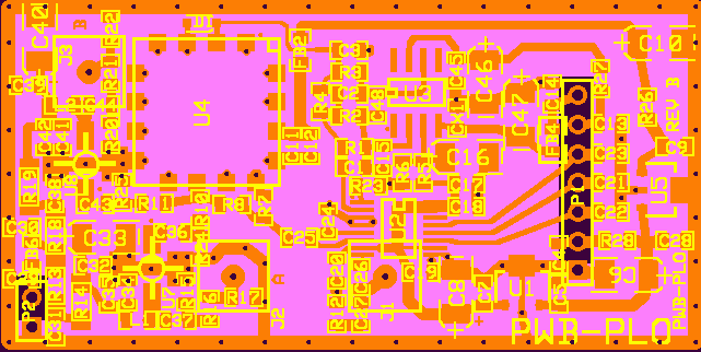
PWB-PLO rev B
Printed Wiring Board for
Phase
Locked
Oscillator
Update 4-30-08,
updated for Revision A
Update 7-23-09,
updated for Revision B
Updated
8-11-09. Update information. Add release
history.
Updated
12-26-10. Update PLL chip support
Printed Wiring Board for Phase
Locked Oscillator,
size-B
Use your mouse's "right click" and "Save Link" to download:
a. PWB-PLO
rev B,
Master Artwork, and Layout, in ExpressPCB software. Use this to
order from Express.
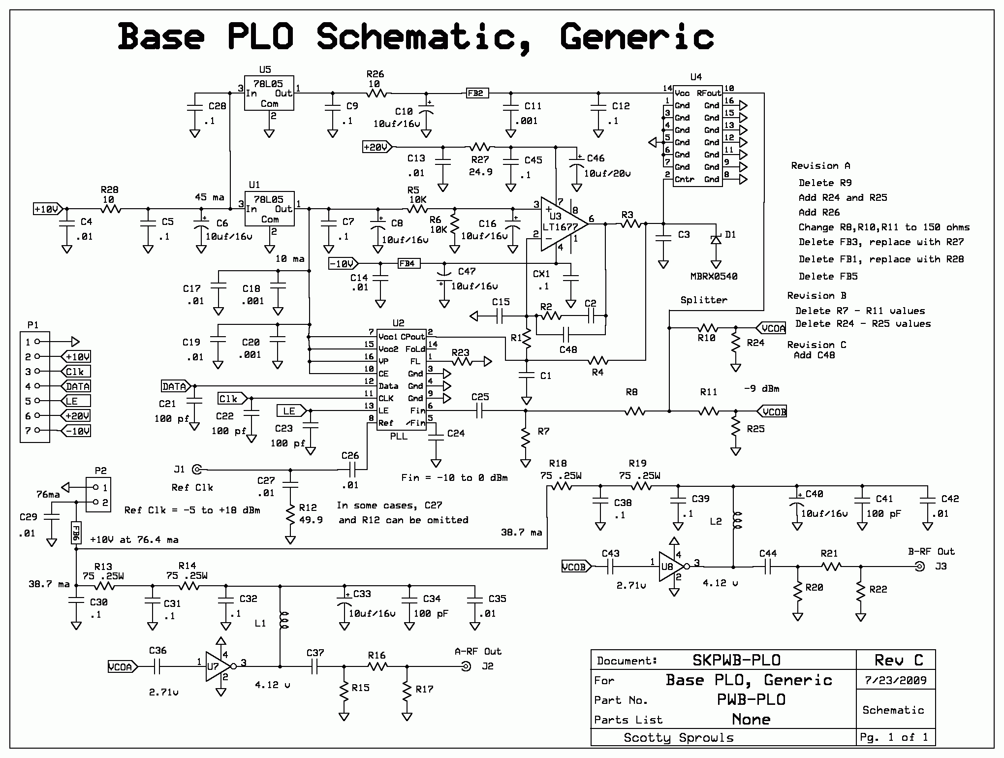
b. SKPWB-PLO
rev C,
Schematic, in ExpressPCB software. Use for reference only.
c. There is no Parts List, since this is a pwb
design,
used to
create SLIM-PLO-xx.
The PWB-PLO is a printed wiring board which is
designed and layed out to contain a PLL, a VCO, and two buffer
amplifiers. There are two types of PLL loops that can be
incorporated. One, as an active loop with
an op amp and a passive loop without an op amp.
Any ROS style VCO can be used. Even a +12v VCO
can be operated at +10v, which is the nominal input voltage.
Although these PLO's are designed with the Minicircuits
ROS style VCOs, many other manufacturer's VCOs will work just as
well.
If an active op amp loop filter is used with a
negative supply voltage, it is likely that the control voltage will go
negative. Many VCO's will stop oscillating with a negative
control voltage of -0.6 volts or greater. This will cause the PLL
loop to "hang". To prevent this situation, a "protection" diode,
D1, is installed on the control voltage line. The voltage will
never go less than -0.4 volts. This will assure that the VCO will
continue to oscillate. This diode must be deleted for all other
configurations.
If a VCO requires +10 volts, the Regulator U5 is not
installed. It is bypassed with a jumper wire or a zero ohm
resistor.
Updated
12-26-10. These PLL chips are supported:
The LMX2326 is the original design but has now become obsolete. The
ADF4118 is a "drop-in" replacement. The ADF4112 or ADF4113 is an
option, requiring the use of R23 (4.7 Kohm). The LMX2326 or ADF4118
does not require
R23.
RF energy from the VCO is divided, 3 ways. The
VCO output power level depends on the VCO used. The Minicircuits
ROS-2150VW and ROS-1500 output a minimum of +5 dBm. One
leg of the divider returns to the PLL for reference locking. We
would like a level of -5 dBm to -10 dBm to drive the PLL chip.
The other two legs are
amplified by U7 and U8 MMIC amplifiers. They can be a variety of
MMICs. I have chosen the Minicircuits ERA-33 because I am using
it in the I.F. Amplifier SLIM and quantity purchases keep the cost
low. The level of RF output is determined by several
factors. VCO type,
the amount of resistive attenuation in the 3-way splitter, the MMIC
amplifier used, and the amount of resistive attenuation placed
in the output
paths. The typical maximum output is +13 dBm.
When the PLO is used as a wide band frequency source
to drive the LO port of a mixer, the buffer
amplifiers are operated in, or close to, saturation. This may
seem like a bad idea, but it does two things. First, the
output level will have minimum ripple across it's frequency
range. Second, the non-harmonically related, spurious
signals will less than if the linear mode. Normal harmonics will
be higher, but, as a local oscillator for
mixers, it
doesn't matter. I have tested with both the Sirenza SGA-4586 and
the
Minicircuits ERA-33SM. The ERA-33 compression level is a little
"flatter" than the SGA-4586. If linear operation is desired, the
resistor divider (R8-R11) could be modified for lower output.
Presently, there are 2 SLIM PLO's that are designed
using this PWB: SLIM-PLO-1, and SLIM-PLO-2.
I can see these suffixes
growing, as different
PLO's
are
configured and built. PLO's with any frequency range, up to 3000
MHz, can be configured from this Base Design. At one time there
was a SLIM-PLO-3 but it is discontinued.
Release History
Original Release:
Released 7-01-2007
PWB: PWB-PLO Rev 0, archived
Schematic: SKPWB-PLO Rev 0,
released 7-01-2007, archived
Revision A: Released 4-26-2008
PWB: PWB-PLO Rev A, archived
Schematic: SKPWB-PLO Rev A,
released 4-26-2008, archived
Revision A:
1. Revision A changes the R8-R11 VCO
power divider. The new topology adds about 10 dB more isolation
between the buffer amplifiers. It also decreases the drive to the
buffers.
2. Revison A removes the optional component path under
U5. This was a potential short circuit.
3. Revision A changes the input ferite beads to
resistors, to allow for better power supply filtering.
4. Revision A adds R26, for better VCO noise
performance.
The previous board, Rev 0, should be modified for these changes.
Change 1 requires a trace removal to allow repositioning of the R8-R11
change. Change 2 also requires a trace removal.
5. Revision A also changes the pad sizes
for the
electrolytic capacitors so that ceramics can be used as alternate parts.
Revised schematic, 6-11-2008,
delete values to make schematic generic.
PWB: PWB-PLO Rev A
Schematic: SKPWB-PLO
Rev B, archived
Revision B: Released 7-23-2009
PWB: PWB-PLO Rev B
Schematic: SKPWB-PLO Rev C
Revision B adds a feedback capacitor to the
PLL Loop, C48. The Master Layout Artwork was revised to
accommodate the new capacitor. Previous revisions of the PWB can
be
easily modified to allow addition of C48.