SLIM-ADC-12
Analog to Digital
Converter
Updated 12-22-12. Add explanation
for Optional Power
Modification when used with MSA/VNA.
No pwb or schematic changes.
SLIM-ADC-12,
AtoD Converter, 12 bit, size
A
Use your mouse's "right click" and "Save Link" to download:
a. SKSLIM-ADC-12,
Schematic, in ExpressPCB software.
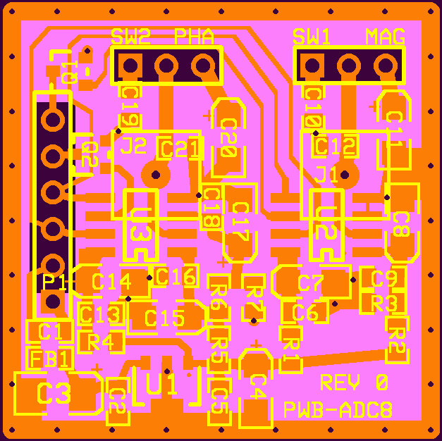
b. PWB-ADC8,
Base
artwork for PWB, in ExpressPCB software.
Use this drawing to order the pwb from Express, or to locate
the parts on the SLIM-ADC-12.
c. PLSLIM-ADC-12
rev A,
Parts List in text format. Open with Exel
or Lotus, etc.
d. Download the AD7685 data sheet at: http://cds.linear.com/docs/Datasheet/18601fa.pdf
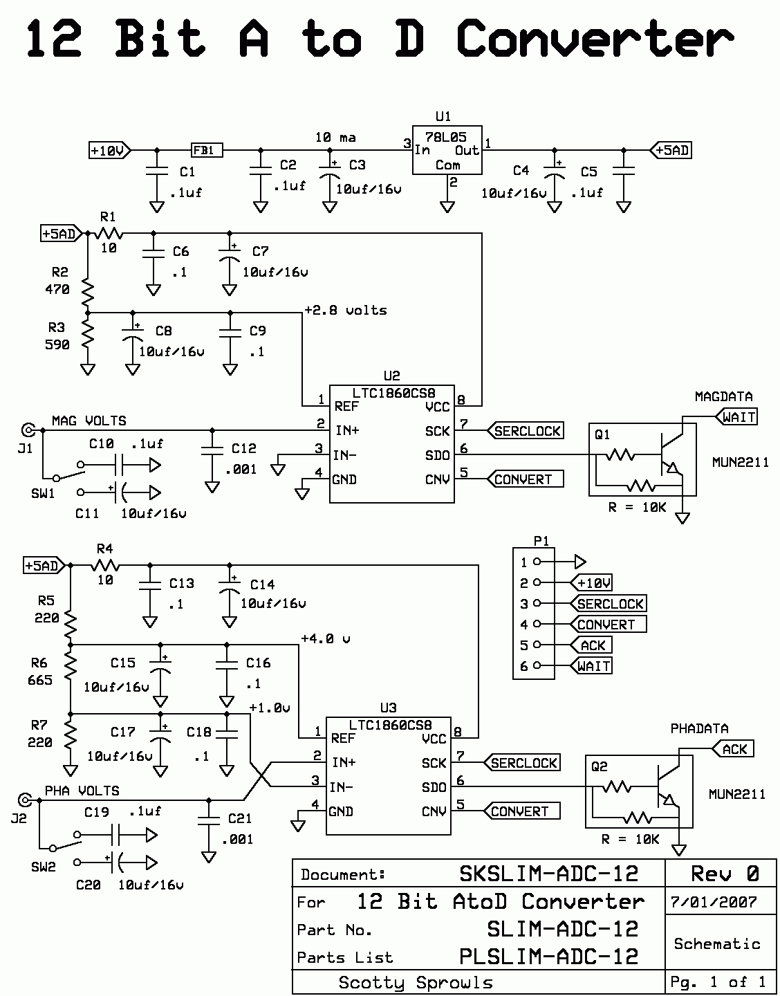
The SLIM-ADC-12 is a dual 12 bit
converter
using the
less expensive LTC1860.
The U2 AtoD
will convert the J1 input of 0 to 2.8
volts for a maximum of 4096 bits. This equates to 684 uv per
bit.
The voltage divider R2 and R3 determine the reference of the AtoD and
can be modified to any value between 1.5 volts and 5.0 volts.
This design sets it to 2.8 volts.
The
U3 AtoD will convert the J2 input of 1.0 volts to 4.0 volts for a
maximum of 4096 bits. This equates to 732 uv per bit. The
voltage
divider R5, R6, and R7 determine the references and therefore, the
minimum and maximum input range of the
AtoD. This voltage divider could also be
modified for specialized inputs.
Updated
11-26-09 Modification of U3 AtoD for a J2
input of 0 volts to 5.0 volts (1.22 mv/bit):
Remove or delete R6.
Change R5 to 10 ohms.
Change R7 to zero ohms. C17 and C18 may be removed or
deleted.
Both A/D's will
capture, and clock out their
data concurrently. The software commands both U2 and
U3 to
begin conversion with a single toggle of the signal, "CONVERT".
12 toggles of the signal, "SERCLOCK", causes the I.C. to
output a serial stream of
12 bits. The SDO outputs of the AtoD I.C.'s have
limited (500 ua) current
capability. Therefore, Q1 and Q2 provide current
sinking to
drive the "WAIT" and "ACK" lines on the LPT port of the Computer.
The Computer's LPT port
is nominally a TTL compatable input with a pull up resistor to
+5 volts.
The circuit is designed with thru hole pads, to
allow each input to be connected
to an external switch. The switch selects the amount of capacitance to
be placed in shunt with the
input. Each switch is a single pole, dual throw, with a
non-connecting center position. This allows a selection of
3
different integration times (Video Bandwidth). This module is
expected to be mounted very close to the front panel of the integrated
system so that the user can mount the switches on the front panel and
maintain very short leads from the switches to the bottom of the module.
The base PWB has the part number,
PWB-ADC8. The "8"
signifies the use of an 8 pin SOIC package. There are other
A/D I.C.s with this package. More A/D SLIMs could be created from
this
design.
Optional Power Modification
to SLIM-ADC-12 when
used in the MSA with VNA
extension:
This optional modification allows the SLIM-ADC-12 to
be powered directly by the Phase Detector Module's regulated +5
volts. This
causes both modules to use the same regulated +5 volts. This
results in more accurate Phase Measurements with the VNA.
The modification is quite simple: Remove and delete
U1, the 78L05. Jumper a wire between the two pads that supported
U1. The pads are U1 pin 3, to U1 pin 1. The power input at
P1 pin 2 must be +5 volts, which is provided by the Phase Detector
Module.
SKSLIM-ADC-12, Schematic of SLIM-ADC-12