Original
Release 5-30-2016.
Revision 0 Update
11-12-2016. Add explanation for installing
AD7685 and LT1864 Update
2-04-2017. Add connections to the MSA SLIM
Control Board Update
2-06-2017. Add *Note for C6. (C6 missing
from PWB)
SLIM-ADCMUX, 8 Channel Analog to Digital Converter,
size-A
Use
your mouse's "right click" and "Save Link" to download:
a.
SKSLIM-ADCMUX.sch
Rev 0,
Schematic, in ExpressPCB software.
b. PLSLIM-ADCMUX Rev 0,
Parts List. Maintained on this page only.
c.
PWB-ADCMUX.pcb
Rev 0 ,
Base
artwork for PWB, in ExpressPCB software.
Use this drawing to order the pwb from Express.
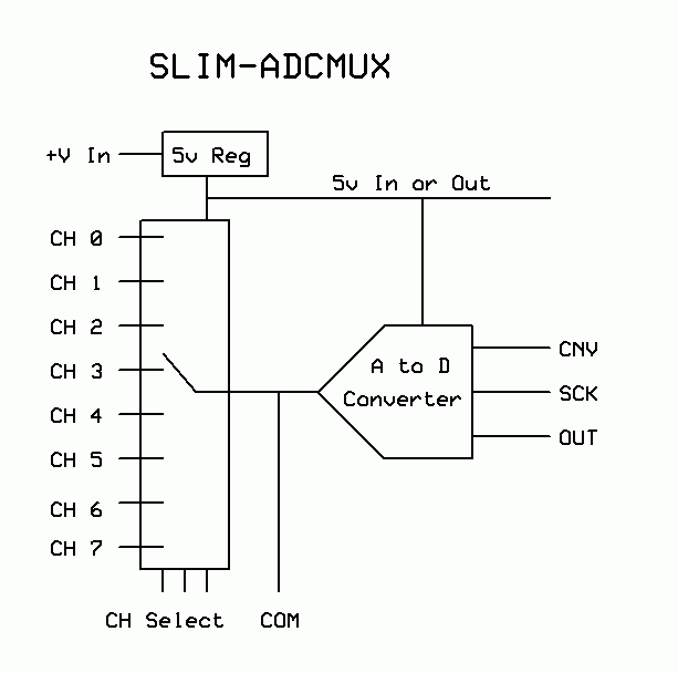
The SLIM-ADCMUX is a selectable, 8 channel, analog
to digital converter (ADC). The circuit is divided into two sections,
an 8 channel analog switch and a serial analog to digital converter.
The SLIM-ADCMUX can be used as an independent 8
channel analog switch by not populating the ADC circuit. Likewise, it
can be used as a single channel ADC by not populating the analog switch
circuit.
The multiplexer is bi-directional,
meaning, a
signal on the multiplexer input will be transferred to the COM
connection or a signal on the COM will be transferred to the
multiplexer's input. The multiplexer IC will pass analog or digital
signals with a bandwidth limitation greater than 20 MHz.
Specifications:
Size: L = 1.2 in, W = 1.2 in, H = 0.5 in.
Supply voltage: +7.0 v. to +15 v. using internal +5v regulator.
(Option, +5v input with no internal regulator.)
Supply Current: less than 5 ma.
Signal input resistance: greater than 1 Meg ohm
Signal input impedance of ADC: Series resistance and capacitance, 3K
ohm and
30 pfd.
Input Signal voltage range: 0v to +5.0v.
Control inputs: 5v CMOS
Serial Output Options:
a. Open Drain. R6 and R7 are not installed.
b. 5v CMOS. R6 installed. R7 is not installed.
c. 3.3v CMOS.
(depends on
R6/R7). Both R6 and R7 are installed.
Acquisition speed: 150 K samples per second, maximum. (The MSA requires
about
1 KSPS)
Resolution Error: +/- 3 bits = +/- 0.23 mv. max. (in the MSA this
equates to plus or minus 0.01 dB or 0.008 degrees)
Note: It is not necessary to shield this module. Whatever noise is
coupled into the circuit, the capacitor C6 will shunt it to ground.
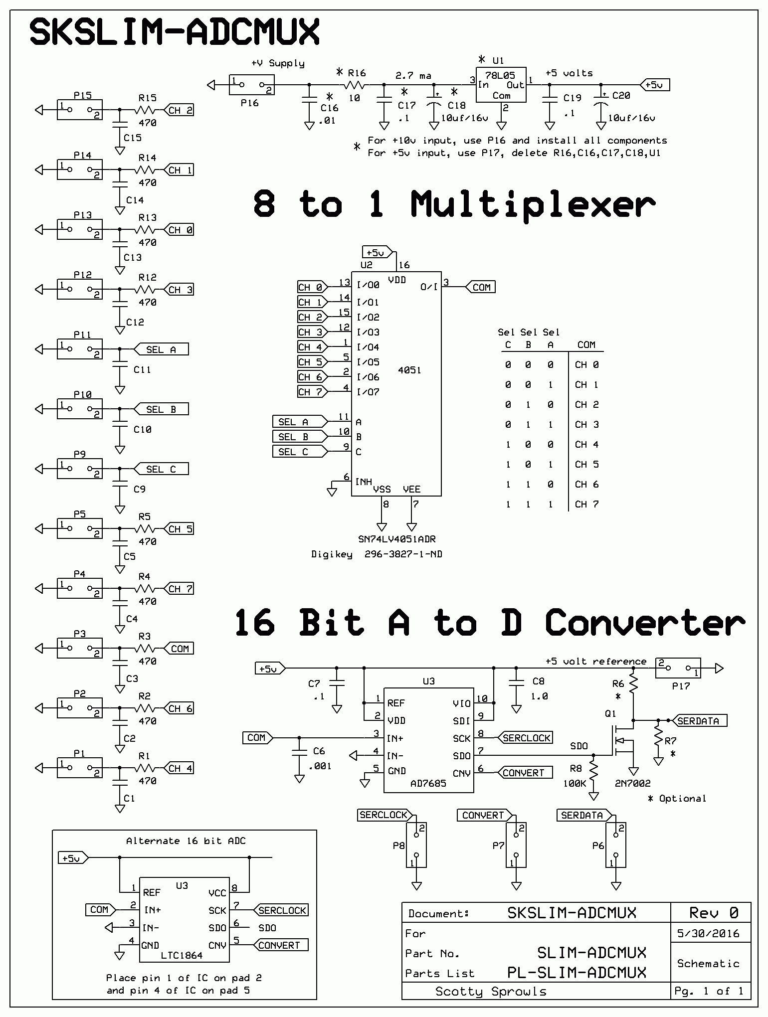
The suggested ADC is either the 16 bit LTC1864, an 8
pin package or the 16 bit AD7685, a 10 pin
package. However, other
ADC's can be used if the IC package will
fit and the command protocall conforms to the pin/pad layout.
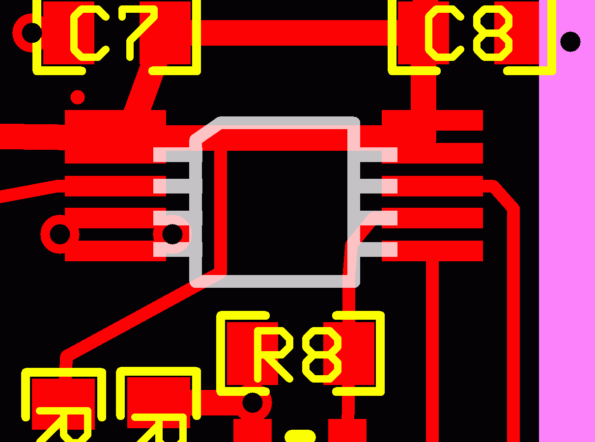
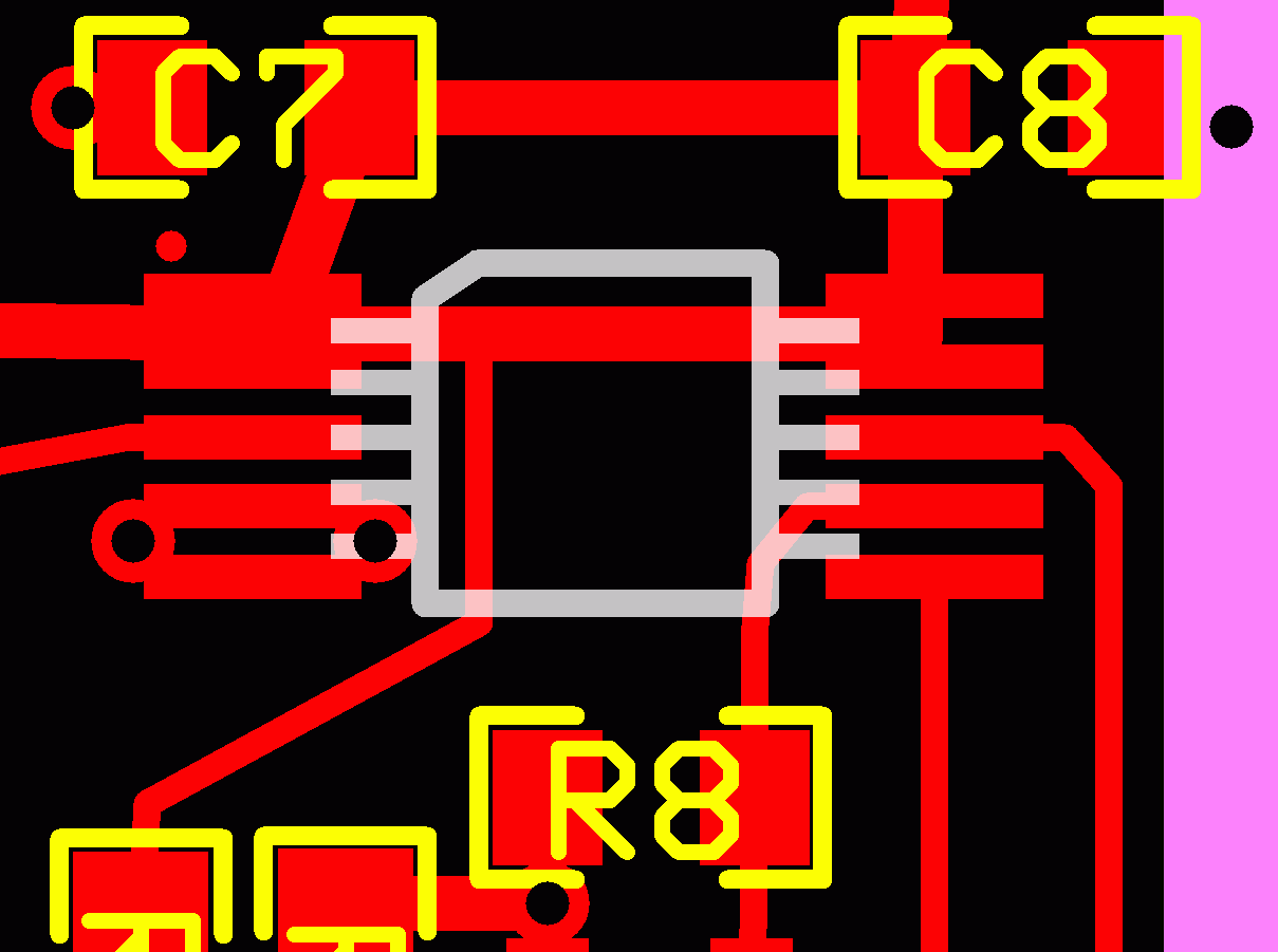
Schematic, SKSLIM-ADCMUX Layout for
SLIM-ADCMUX
The following pictures show how to position the LT1864 and
AD7685 on the available pads at U3.
LT1864
AD7685
When installing the LT1864, position its pin 1 on the pwb pad 2. The
chip's pin 8 is positioned on the pwb pad 9.
The AD7685 requires some of its leads to be bent for correct alignment.
Solder pins 3 and 8 of the chip to the center of the pwb pads 3 and 8.
Slightly bend the pins 4, 5, 6, and 7 of the chip downward to align
with the pwb pads and solder. Slightly bend the pins 1, 2, 9, and 10
of the chip to align with the pwb pads and solder.
Parts List, PLSLIM-ADCMUX Revision 0, 5-30-2016
Des. Value
Part Number
Digikey Number
Cost
Notes
C1 optional
The optional capacitors can be
C2 optional
any value that user deems
C3 optional
necessary for operation.
C4 optional
C5 optional
C6 .001 uF
C0805C102J5GACTU
399-1136-1-ND
0.08 * see Note for C6
C7 .1
uF
C0805C104K3RACTU
399-1168-1-ND
0.08
C8 1.0 uF
C2012X7R1E105K125AB
445-1354-1-ND
0.14
C9 optional
C10 optional
C11 optional
C12 optional
C13 optional
C14 optional
C15 optional
C16 .01 uF
C0805C103K5RACTU
399-1158-1-ND
0.08 * see Power Option
C17 .1 uF
C0805C104K3RACTU
399-1168-1-ND
0.08 * see Power Option
C18
10uf/16v AVX,
TPSB106K016R0500
478-5230-1-ND
0.65 * see Power Option
C19 .1 uF
C0805C104K3RACTU
399-1168-1-ND
0.08
C20
10uf/16v AVX,
TPSB106K016R0500
478-5230-1-ND
0.65
P1 Conn, 2
pin
sold as row of 36 pins
S1012E-36-ND
0.06
P2 Conn, 2
pin
sold as row of 36 pins
S1012E-36-ND
0.06
P3 Conn, 2
pin
sold as row of 36 pins
S1012E-36-ND
0.06
P4 Conn, 2
pin
sold as row of 36 pins
S1012E-36-ND
0.06
P5 Conn, 2
pin
sold as row of 36 pins
S1012E-36-ND
0.06
P6 Conn, 2
pin
sold as row of 36 pins
S1012E-36-ND
0.06
P7 Conn, 2
pin
sold as row of 36 pins
S1012E-36-ND
0.06
P8 Conn, 2
pin
sold as row of 36 pins
S1012E-36-ND
0.06
P9 Conn, 2
pin
sold as row of 36 pins
S1012E-36-ND
0.06
P10 Conn, 2
pin
sold as row of 36 pins
S1012E-36-ND
0.06
P11 Conn, 2
pin
sold as row of 36 pins
S1012E-36-ND
0.06
P12 Conn, 2
pin
sold as row of 36 pins
S1012E-36-ND
0.06
P13 Conn, 2
pin
sold as row of 36 pins
S1012E-36-ND
0.06
P14 Conn, 2
pin
sold as row of 36 pins
S1012E-36-ND
0.06
P15 Conn, 2
pin
sold as row of 36 pins
S1012E-36-ND
0.06
P16 Conn, 2
pin
sold as row of 36 pins
S1012E-36-ND
0.06
P17 Conn, 2
pin
sold as row of 36 pins
S1012E-36-ND
0.06
R1 470 ohm
MCR10ERTF4700
RHM470CHCT-ND 0.04
R2 470 ohm
MCR10ERTF4700
RHM470CHCT-ND 0.04
R3 470 ohm
MCR10ERTF4700
RHM470CHCT-ND 0.04
R4 470 ohm
MCR10ERTF4700
RHM470CHCT-ND 0.04
R5 470 ohm
MCR10ERTF4700
RHM470CHCT-ND 0.04
R6
2.2K
MCR10ERTF2201
RHM2.20KCHCT-ND
0.04 * Optional Pull-up for CMOS or TTL
output
R7 4.02K
MCR10ERTF4021
RHM4.02KCHCT-ND 0.04 * Optional
Pull-down for 3.3v output
R8
100K
MCR10ERTF1003
RHM100KCHCT-ND
0.04
R12 470 ohm
MCR10ERTF4700
RHM470CHCT-ND 0.04
R13 470 ohm
MCR10ERTF4700
RHM470CHCT-ND 0.04
R14 470 ohm
MCR10ERTF4700
RHM470CHCT-ND 0.04
R15 470 ohm
MCR10ERTF4700
RHM470CHCT-ND 0.04
R16 10 ohm
MCR10ERTF10R0
RHM10.0CHCT-ND
0.04 * see Power Option
Q1 2N7002 FET
2N7002-7-F
2N7002-FDICT-ND
0.15
U1 78L05
78L05ACU
497-1183-1-ND
0.77 * see Power Option
U2 74LV4051 SN74LV4051ADR
296-3827-1-ND
0.45
U3
AD7685
AD7685BRMZ
AD7685BRMZ-ND
16.16
U3-alternate LTC1864IMS8#PBF
LTC1864IMS8#PBF-ND
13.57 * alt U3
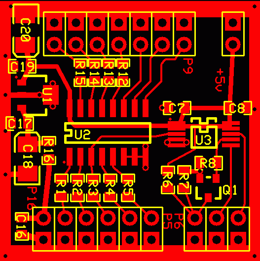
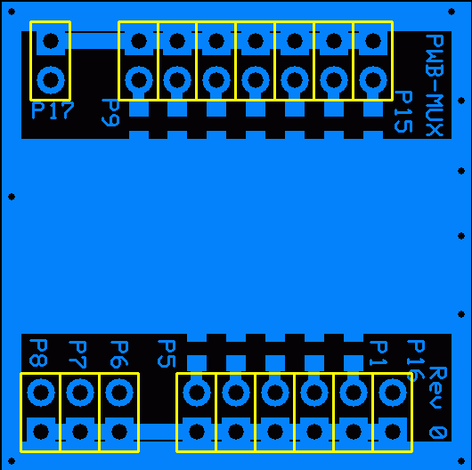
PWB Circuit Board
PWB-ADCMUX
3.28
* alt U3 is Linear Technology LT1864, an 8 pin package. Its
pin 1
is placed on the pwb's pad pin 2. Its command protocall is the same as
the AD7685.
* Power Option: The
SLIM-ADCMUX can be powered
one of two ways:
1. Application of +7.0 volts to +15 volts onto P16. The internal
regulator will output +5 volts (+/- .1 v) onto P17. The voltage at P17
can then be used to power the final stage of the SLIM-PDM. This will
assure that the PDM signal and the Analog to Digital Converter will
have the same reference voltage. This assures maximum accuracy for VNA
Phase measurements.
Or,
2. The internal +5 volt regulator is not configured and a +5 volt
source is applied to P17. For the MSA/VNA, The +5 volts at
the final stage of the SLIM-PDM, P2, is used to supply power to P17. Do
not
install R16,C16,C17,C18, and U1
In either case, this will assure that the PDM signal
and the Analog to Digital
Converter will have the same reference voltage. This assures maximum
accuracy for VNA Phase measurements.
* Note for C6. The PWB-ADCMUX
Rev 0 is missing component pads to accomodate C6. On the
bottom of the board are pads to add the optional capacitors for each
input. P3-2 is the common connection for use as an input to the ADC or
as an output from the Mux. The capacitor on this point is C3.
If the board is used as a Multiplexer + ADC (which replaces the
original SLIM-ADC), then make R3 zero ohms and make C3 .001 ufd. That
will satisfy the missing C6.
The connections from the Control Board are:
CB
ADC-MUX
P3-2 (P3D0) to P11-2 (Sel A)
P3-3 (P3D1) to P10-2 (Sel B)
P3-4 (P3D2) to P9-2 (Sel C)
P3-1 Gnd to
P9-1 Gnd
P3-8 (P3D6) to P8-2
(SERCLOCK)
P3-9 (P3D7) to P7-2
(CONVERT)
P25-4 (WAIT) to P6-2 (SERDATA)
P25-1 Gnd
to P6-1 Gnd