Modularized Spectrum Analyzer
(do a browser "refresh" to make sure this is the latest update)
This
Page was
Started Oct. 3,
2010 If you have comments or
suggestions, I will be happy to hear about them.
Scotty. [wsprowls (a.t.) yahoo.com]
Updated Oct. 10, 2010 Added more information to Master Oscillator Voltage Tests
Updated Dec. 25, 2012 Changed Cavity Filter sweep test (available with MSA Software version 116)
You can link to a specific SLIM's web page by clicking on the module's paragraph header. Here are other links supporting the MSA :
Main Page for MSA Main page for the MSA.
Construction page for the SLIM MSA.
The purpose of this page is to help the MSA builder test a fully integrated MSA using minimum test equipment. I have written this page with a VOM (Volt-Ohm-Meter) as the primary piece of test equipment. In some cases of troubleshooting, higher level test equipment will be required, but I will try to keep it as simple as possible.
There are three reasons to use the procedures on this page.
1. Your MSA is functioning correctly and you just want to verify operations to get that "warm fuzzy feeling". For this, use the Verification Procedure.
2. Your MSA is not functioning within its specified capabilites. For this, use the Verification Procedure.
3. Your MSA is not operating at all, a "Hard Failure". For this, use the Troubleshooting Guide.
For any reason, this page consists of multiple tests that will verify the operation of each SLIM within a completed MSA/TG/VNA. This page is composed of four sections.
I. Troubleshooting Guide
A step-by-step procedure to help find a "Hard Failure" in the MSA. A "Hard Failure" is when the MSA is not operating at all. If the MSA is not performing to its specifications, it is considered a "Soft Failure" and it is more appropriate to follow the Verification Procedure to fix the problem.
II. Verification Procedure
Step-by-step procedures to verify the full functionality of the MSA. If a failure is encountered in these steps, it will refer you to perform a separate test in one, or both, of the next two sections.
III. SLIM Voltage Tests
Step-by-step procedures to measure and verify operating voltages within each SLIM of the MSA.
IV. Dynamic Signal Tests
Step-by-step procedures to allow the tester to minipulate signals that verify operation of the SLIMs.
This page is most relevant for an MSA using the "Direct Coaxial Connection" method of attaching RF cables, or for a connectorized MSA when the builder wishes to test or troubleshoot with minimal RF cable disconnections. For either, it is assumed that the MSA is completely integrated with all SLIMs and the wiring harness is completely inter-connected. Disregard testing of modules not present. If your MSA is partially integrated and is using RF connectors, refer to the page, Test-As-You-Build.
Items Required for Testing the Integrated MSA:
1. Completely integrated Basic MSA, MSA with Tracking Generator, or MSA/VNA
2. External DC power supply or wall wart rated at a nominal +13.6v, 1000 ma.
3. Computer with LPT port (parallel printer port) or Cypress USB Board interface.
4. Volt-Ohm Meter (VOM, Digital or Analog). All voltage measurements are DC unless noted.
5. Optional Oscilloscope, but may be necessary for troubleshooting a faulty module.
6. Software: MSA Program as spectrumanalyzer.exe (executable) or spectrumanalyzer.bas (Liberty Basic)
Set-Up, common for all testing on this page:
1. It is assumed that the MSA Software has been downloaded from the MSA Web Site and has been initialized. If not, go to the Web Page: Initial Set Up and Calibration. Follow the instructions for inital running of the MSA Software. You can run the ".bas" application with Liberty Basic as the main program, or the ".exe" application without Liberty Basic.
2. Apply power (+13.6 v nominal) to the Control Board. The Control Board supplies the necessary voltages to the other SLIMs in the MSA.
3. Connect the Control Board LPT connector to the Parallel Port of the Computer or the USB Interface.
4. Most of the tests will ask you to "Run the MSA Program". The MSA Main Graph will open and sweep with the MSA in the Spectrum Analyzer mode, 1G Band. An operational MSA will sweep with the Magnitude trace indicating the Final Crystal Filter response centered at (or near) "0 MHz".
I. Troubleshooting Guide for the MSA
Hard Failures for Basic MSA
A "Hard Failure" is when the MSA is not operating at all. The Magnitude trace will be flat, with no remarkable pattern, and will be at one of three levels: 0 dBm, -120 dBm, or in between 0 and -120 (probably about -100 dBm).
Set-Up for Troubleshooting a Hard Failure
1. Run the MSA Program. The MSA Main Graph will open and sweep with the MSA in the Spectrum Analyzer mode, 1 G Band, Path 1.
2. If entering the Troubleshooting after the initial "turn-on" of a newly completed MSA, Path 1 has default calibration values: 0 bits = -120 dBm, 32767 bits = 0dBm. This is fine.
3. Video Filter to Wide.
4. If not previously done, Halt the sweep, open the Magnitude Scale Window (Axis Y2 Window), and change the Top Ref to 0 and the Bot Ref to -120. Click "OK", the Window will close.
5. Open Variables Window (under Menu, Options) to display Magdata (dBm) and magpower (bits).
6. Click "Restart".
If the Magnitude (magpower) is a flat trace at -120 dBm or at 0 dBm (and Magdata = 65534 or 0), there is a high probability that the failure can be attributed to one of the following (in order of testing): Computer (addressing), Control Board, A to D Converter Module, and Log Detector Module (or their interconnecting wires or cables). If the Magnitude is a flat trace (with a little noise) somewhere between -120 dBm and 0 dBm, the failure will more likely be attributed to one of the other modules (or their interconnecting wires or cables). Testing will continue in the following order: PLO 2, DDS 1, PLO 1, Master Oscillator, I.F. Amplifier, Final Crystal Filter, and Coaxial Cavity Filter.
Procedure for Troubleshooting a Hard Failure
Test your MSA in the following order. Once a problem is determined and fixed, the Magnitude trace should revert to a normal level. If it doesn't, continue with the procedure until it does.
Computer (hardware)
Verify your computer Status lines are pulled up via computer or Control Board. A failure here will indicate that the computer can not "listen" to the Control Board.
a. Measure the voltage at Control Board, LPT, pin 12 and pin 13. Must be greater than + 2.0 volts.
If it is not, you must add the pull-up resistors, R9 through R12 on the Control Board or on the Cypress USB board.
Computer (addressing)
Verify "Port" signals are active, to assure Computer is "talking".
a. Measure the "Port" signal on the Control Board, using a voltmeter (Contol Board ground to LPT-2).
This is an active TTL clock signal and measured voltages will vary. However,
* a DC voltage reading should be between +.3 and +2.0 volts. If it is, continue at step 2.b.
* A 0 volt reading indicates a problem with the computer or LPT cable,
* remove the LPT cable from the computer and repeat the measurement directly on
the Parallel Port connector (pin 2 is "Port", pin 25 is ground). If good here, but not on the
Contol board, the LPT cable is bad. If not good here,
* the Port Address is incorrect for your Parallel Port interface.
* Determine correct Parallel Port Address. Install it in the Hardware Configuration Manager.
Control Board
Verify "Control" and "Port" signals are active, to assure Control Board is "listening".
a. Measure the "Port" signal at Control Board, P1-2 (common CLK to other modules)
* This is an active CMOS clock signal and measured voltages will vary, however
* a DC voltage reading should be between +.3 and +2.0 volts
* if it is, the computer and Control Board are operating.
* a 0 volt reading indicates a problem with the Control Board,
* go to the section, SLIM Voltage Tests and perform the paragraph, Control Board.
A to D Converter Module
This is the only portion of the MSA that "talks" to the computer.
a. Go to section, SLIM Voltage Tests, and perform the paragraph, A to D Module.
b. Go to section, Dynamic Signal Tests, and perform the paragraph, A to D Converter Signal Test.
Log Detector Module
a. Go to section, SLIM Voltage Tests, and perform the paragraph, Log Detector Module.
b. Go to section, Dynamic Signal Tests, and perform the paragraph, Log Detector Signal Test.
IF Amplifier Module
a. Go to section, SLIM Voltage Tests, and perform the paragraph, I.F. Amplifier Module.
b. Go to section, Dynamic Signal Tests, and perform the paragraph, I.F. Amplifier Noise Test.
Master Oscillator Module
a. Go to section, SLIM Voltage Tests, and perform the paragraph, Log Detector Module.
b. Go to section, Dynamic Signal Tests, and perform the paragraph, Master Oscillator Signal Test.
PLO 2 Module
a. Go to section, SLIM Voltage Tests, and perform the paragraph, PLO 2 Module.
DDS 1 Module
a. Go to section, SLIM Voltage Tests, and perform the paragraph, DDS Module.
b. Go to section, Dynamic Signal Tests, and perform the paragraph, DDS Command Test, and
c. go to section, Dynamic Signal Tests, and perform the paragraph, DDS 1 Signal Test.
PLO 1 Module
a. Go to section, SLIM Voltage Tests, and perform the paragraph, PLO 1 Module.
Final Crystal Filter
a. Go to section, Dynamic Signal Tests, and perform the paragraph, Final Crystal Filter Test.
Coaxial Cavity Filter
a. Go to section, Dynamic Signal Tests, and perform the paragraph, Coaxial Cavity Filter Test.
DDS 3 Module (if installed)
a. Go to section, SLIM Voltage Tests, and perform the paragraph, DDS Module.
b. Go to section, Dynamic Signal Tests, and perform the paragraph, DDS Command Test, and
c. go to section, Dynamic Signal Tests, and perform the paragraph, DDS 3 Signal Test
PLO 3 Module (if installed)
a. Go to section, SLIM Voltage Tests, and perform the paragraph, PLO 3 Module.
Phase Detector Module (if installed)
a. Go to section, SLIM Voltage Tests, and perform the paragraph, Phase Detector Module.
Soft Failures
A "Soft Failure" is when the MSA is not performing to specification. Use the Verification Procedure.
II. Verification Procedure
Test Sequence for Verification:
Voltage Tests
Go to the section, SLIM Voltage Tests and, for the:
1. Control Board, perform the paragraph, Control Board.
2. Analog to Digital Converter, perform the paragraph, A to D Module.
3. Log Detector, perform the paragraph, Log Detector Module.
4. Master Oscillator, perform the paragraph, Master Oscillator.
5. I.F. Amplifier, perform the paragraph, I.F. Amplifier Module.
6. DDS 1, perform the paragraph, DDS Module.
7. PLO 2, perform the paragraph, PLO 2 Module.
8. PLO 1, perform the paragraph, PLO 1 Module.
9. DDS 3, perform the paragraph, DDS Module, (if installed)
10. PLO 3, perform the paragraph, PLO 3 Module, (if installed)
11. Phase Detector, perform the paragraph, Phase Detector Module, (if installed)
Performance Tests
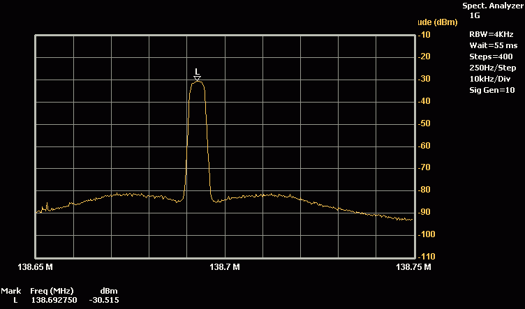
12. Perform the "Zero" Frequency Sweep Test. Compare the data of your MSA to the data given in the test procedure to determine the performance of your MSA.
a. During this test, determine if the L.O. power at Mixer 2 is adequite:
* In Mixer 2, short over the attenuation resistor, R5. This increases the LO power by 1.3 dB.
* If the final Magnitude measurement increases by more than .5 dB, the mixer is "starved" and
steps should be taken to increase the RF power at Mixer 2, J1.
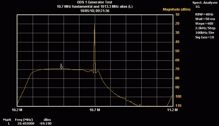
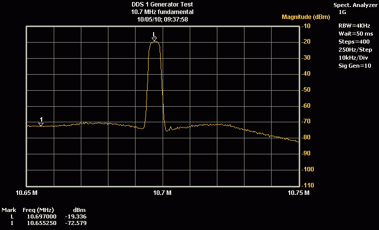
13. Perform the DDS 1 Generator Test. This is a good indication of the measurement accuracy of the Spectrum Analyzer at 10.7 MHz.
a. During this test, determine if the L.O. power at Mixer 1 is adequite:
* In Mixer 1, short over the attenuation resistor, R5. This increases the LO power by 1.3 dB.
* If the final Magnitude measurement increases by more than .5 dB, the mixer is "starved" and
steps should be taken to increase the RF power at Mixer 1, J1.
14. Perform the I.F. Amplifier Signal Test.
15. If your Final Crystal Filter is removable, perform the Optional Coaxial Cavity Filter Test. This test will indicate the general "health" of the Coaxial Cavity Filter.
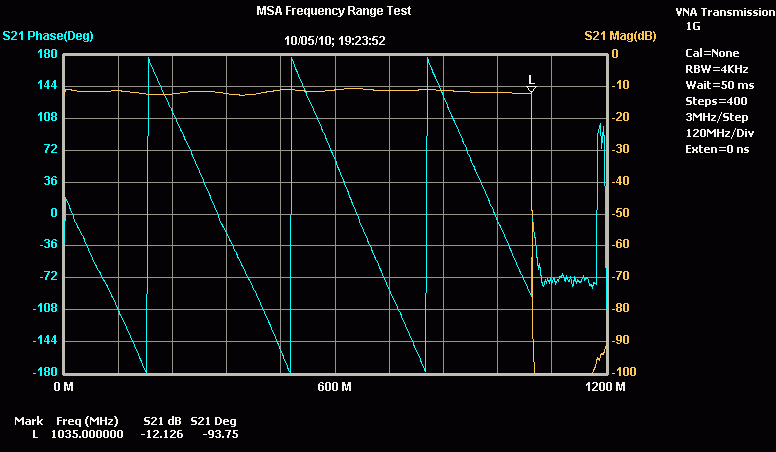
16. For the MSA with Tracking Generator, perform the MSA Frequency Range Test.
Block Diagram for the MSA/VNA
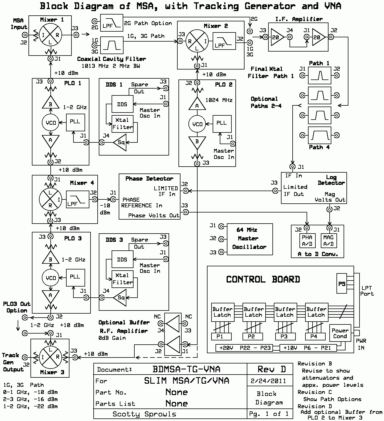
The block diagram shows typical power levels, but not all due to the builder's preference of internal attenuators. Listed here are measured values from the Verification SLIM MSA:
a. Gains = +40 dB (I.F. Amplifier)
b. Losses:
* Mixer 1 conversion loss = -6.5 dB, with - 4.7 dB of attenuator at J2 = -11.2 dB
* L to R port isolation of Mixer 1 = -35 dB, +/- 10.0 dB
* Coaxial Cavity Filter insertion loss = -5.3 dB
* Mixer 2 conversion loss = -6.5 dB
* Path 1 Resolution Filter insertion loss = -4 dB, +/- 1.0 dB
* Mixer 3 conversion loss = -6.5 dB, with - 14 dB of attenuator at J3 = -20.5 dB
* Mixer 4 conversion loss = -6.5 dB, with - 14 dB of attenuator at J3 = -20.5 dB
c. Total gain of Spectrum Analyzer chain, from MSA input to Log Detector input = +13.0 dB
d. Tracking Generator output power = -10.5 dBm, at 100 MHz.
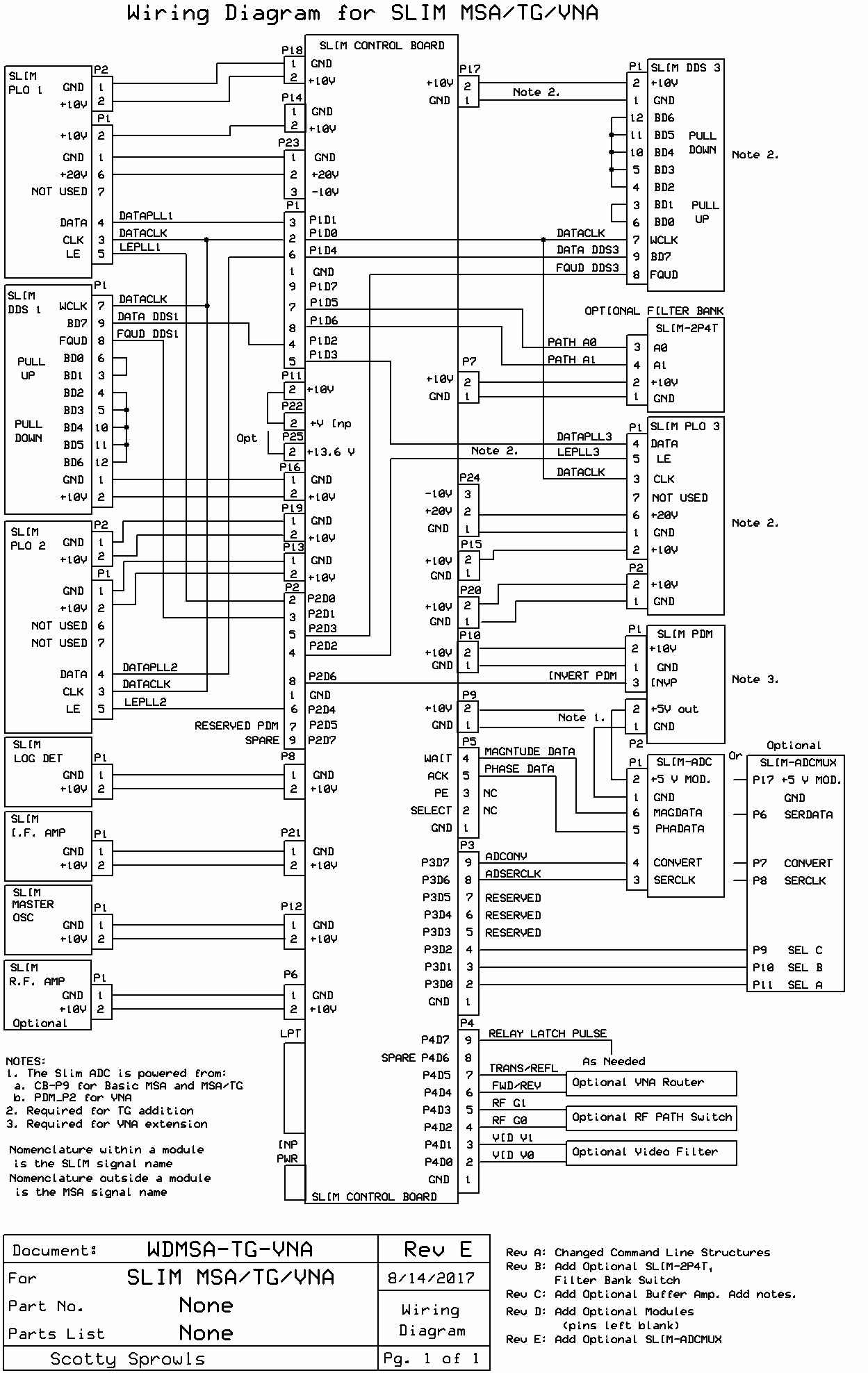
Wiring Diagram for the MSA/VNA
III. SLIM Voltage Tests
The following Test Paragraphs are voltage measurements within each SLIM. Voltages that are out of tolerance will usually indicate a problem within that module. Click the paragraph header to link to the SLIM's web page.
Control Board
The Control Board contains all of the interfacing between the computer and the individual SLIM modules. It also contains the voltage regulation needed for the other modules. The Control Board requires +12 volts to +18 volts DC at 1 amp of peak current. For full MSA operation, the Control Board will use and pass on about 750 ma.
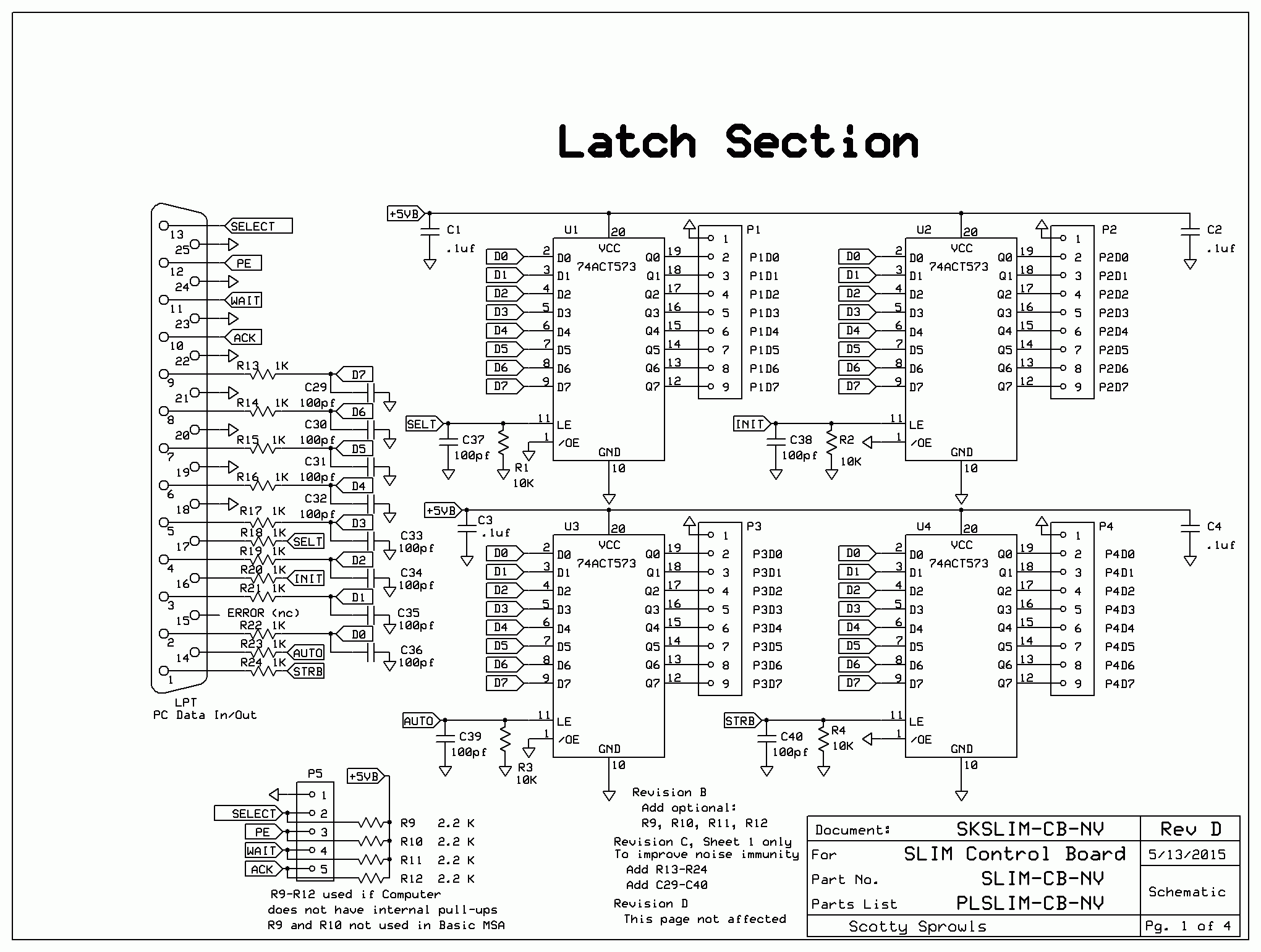
This is the latest schematic of the MSA Control Board. If your Control Board is an earlier version, you will want to test if pull-up resistors are required for your computer. Most home computers do not need them.
Test Procedure:
1. Measure the voltage at these locations, as indicated in the schematic:
a. SELECT and PE. The voltage should read a minimum of 2.0 volts, maximum of 5.0 volts. If you read less than the minimum voltage, remove power, disconnect from the computer and add the pull-up resistors, R9-R12.
b. WAIT and ACK. The voltage should read either a "zero" or "one". A "zero" is 0 volts +.2v. A "one" should read a minimum of 2.0 volts, a maximum of 5.0 volts. If you read less than the minimum voltage, remove power, disconnect from the computer and add the pull-up resistors, R9-R12.
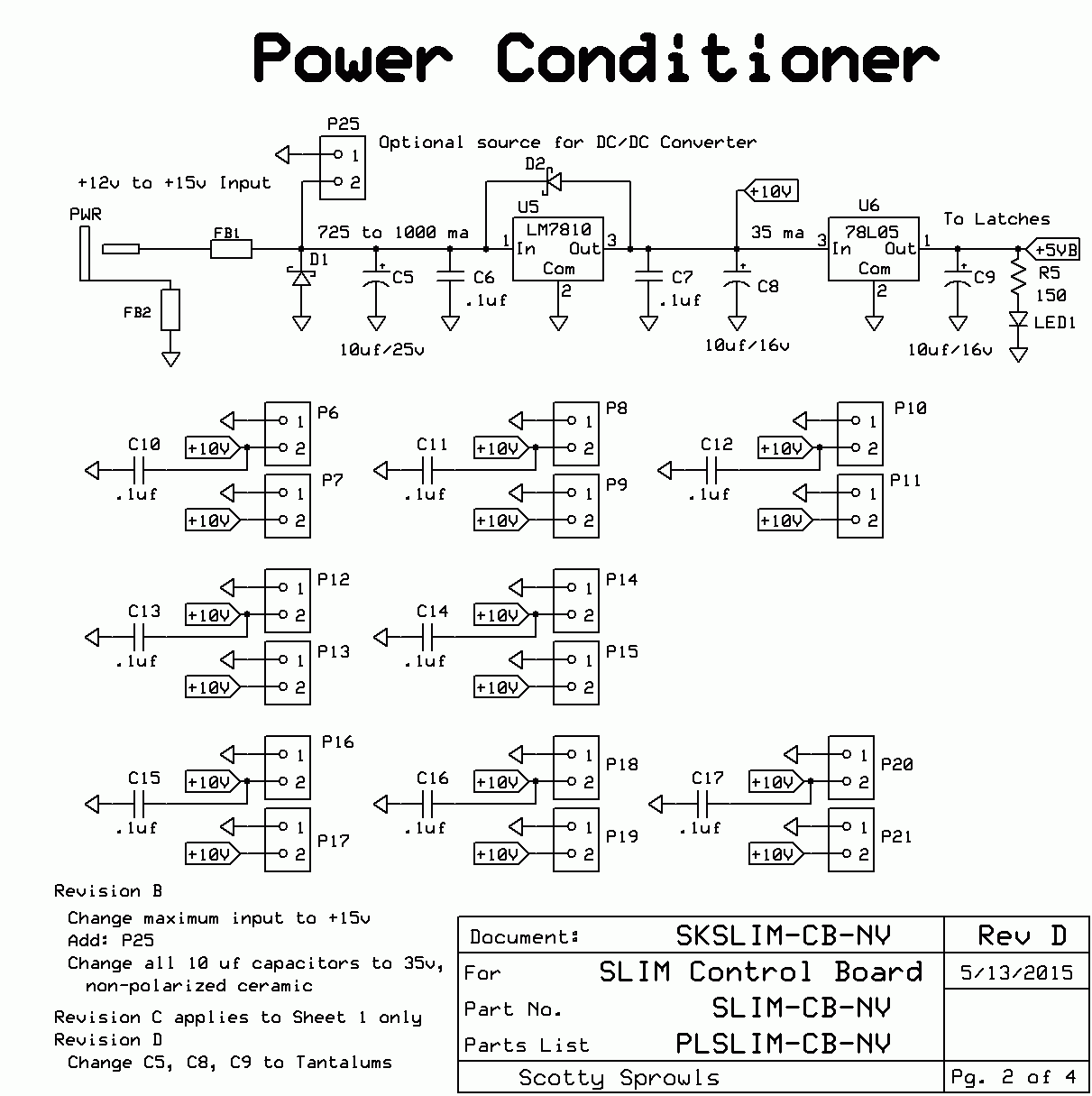
2. Measure the input voltage to the Control Board at U5-1. Range: +12.0 v to +18 v.
3. Measure the output of the +10 volt regulator, U5-3. It should be +10.0 volts, +/- 0.2 volts.
4. Measure the output of the +5 volt regulator, U6-1. It should be +5.0 volts, +/- 0.2 volts.
5. LED 1 should be lit.
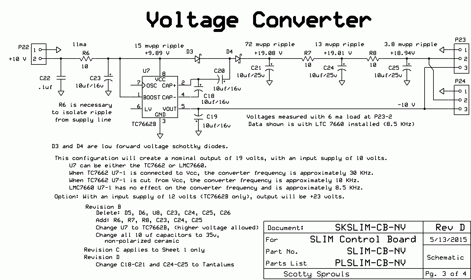
6. Measure the output of the +20 volt multiplier at P23-2 and P24-2. It should be +18.94 volts +/- .3 volts.
7. If you have an oscilloscope, measure the peak to peak ripple at P23-2 or P24-2. It should be less than 20.0 millivolts. When the MSA is completed, excessive ripple will be seen as side bands on every signal when in the Spectrum Analyzer Mode. A cure is too add more capacitance at C20, C21, C23, C24, and C25.
8. If C15 is installed, measure the -10 volt multiplier at P23-3 and P24-3. It should be -10.0 volts, +/- 0.3 volts. The -10 volts is not used in the SLIM MSA, but can be utilized for external experiments requiring current less than 20 ma.
AtoD Module
The following is written for the SLIM-ADC-16. The procedure is the same when using the SLIM-ADC-12.
This test depends on the following other modules connected and operating correctly: Control Board
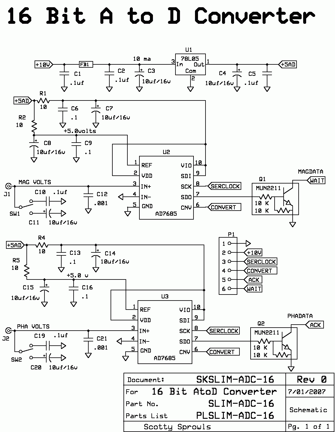
This schematic shows the U1 regulator installed. This is the case for the Basic MSA. For the VNA, it may be ommitted and there must be a jumper wire from the pwb pads of U1-3 to U1-1. Power is supplied from the PDM module's J2-1 and J2-2 to the AtoD module's J1-1 and J1-2. The name "+10v" should be changed to "+5v". Make certain that the PDM module has its ferrite jumpers installed (FBx and FB2).
Test Procedure
1. For the Basic MSA, verify the voltage at U1-3 is +10 volts, +/- .2 volts. For the VNA (no U1) verify the voltage is +5.0 volts, +/- .1 volts.
2. Measure the +5 volts at U1-1, U2-1, U2-2, U2-9, U2-10. It should be +5.0 volts, +/- .1 volts.
3. Measure the +5 volts at U3-1, U3-2, U3-9, U3-10 (if U3 if installed). It should be +5.0 volts, +/- .1 volts. U3 may not be installed for the Basic MSA version.
4. Halt the sweep.
5. Measure the voltage at U2-3. This is the Magnitude output voltage of the Log Detector Module. Its voltage level depends entirely upon the amount of RF power applied to J1 of the Log Detector Module. The voltage should read between +.3 volts and +2.5 volts. A 0 volts reading might indicate a short or low resistance path to ground. A much higher voltage might indicate a short or low resistance path to +5v. If so, inspect for shorts or cleanliness.
6. The voltage at U3-3, if installed, is the Phase output voltage of the Phase Detector Module. Its voltage level is relevant only during a normal VNA set-up condition. However, a 0 volts reading might indicate a short or low resistance path to ground. A +5 volts reading might indicate a short or low resistance path to +5v. If so, inspect for shorts or cleanliness. This voltage will be more critically tested in a later paragraph.
Log Detector Module
The Log Detector Module, SLIM-LD-8306, converts RF power to voltage in a logarithmic function. The bandwidth of the module is 2 MHz to 160 MHz, although the input will be 10.7 MHz in the MSA.
The J2 output is the Magnitude voltage output which goes to the AtoD Module. Its J1 input dynamic range is from approximately -90 dBm to +10 dBm, although this range might be extended. Its J2 output voltage over this range is approximately .35 volts to 2.35 volts.
The J3 output is an RF Limited output of the input frequency. It supplies the Signal Input to the PDM Module (VNA only). The module does not require any direct commands from the computer, and it can be partially tested with only a voltmeter.
This test depends on the following other modules connected and operating correctly:
Control Board, A to D Module
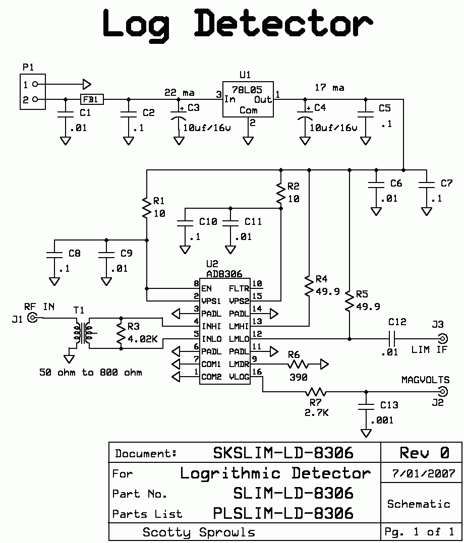
*Note: You may modify the Log Detector Module for AC coupled input by cutting the trace between J1 and the input to transformer T1 and adding a series capacitor (.1 ufd). You may leave the capacitor in place without affecting the characteristics of the Log Detector.
Test Procedure:
1. Verify the voltage at U1-3 is +10 volts, +/- .2 volts.
2. Measure the +5 volts at U1-1. It should be +5.0 volts, +/- .1 volts.
3. Measure the +5 volts at U2-2 and U2-8. It should be about 92 millivolts less than the voltage measured at U1-1.
4. Measure the +5 volts at U2-15. It should be about 64 millivolts less than the voltage measured at U1-1.
5. Measure the voltage at U2-9. It should be +.41 volts, +/- .05 volts if R6 is 390 ohms.
6. Measure the voltage at U2-12 and U2-13. They should be about 25 millivolts less than the voltage measured at U1-1. This is the Limited I.F. output and can be observed with an optional 20 MHz o'scope. With no input signal to the Log Detector, either pin should be about 60 mv peak to peak noise. If a signal is input to the Log Detector, either pin should be about 60 mv peak to peak square wave. If the PDM is connected to J3 of the Log Detector Module, the peak to peak value at U2-12 will be one half that, or 30 mv pp.
7. Measure the voltage at U2-16 and J2. This is the Magnitude output voltage of the Log Detector Module. Its voltage level depends entirely upon the amount of RF power applied to J1 of the Log Detector Module. The voltage should read between +.3 volts and +2.5 volts. A 0 volts reading might indicate a short or low resistance path to ground. A much higher voltage might indicate a short or low resistance path to +5v. If so, inspect for shorts or cleanliness.
Master Oscillator Module
The Master Oscillator Module, SLIM-MO-64, incorporates a 64 MHz crystal oscillator and 3 buffers for distribution to the other SLIMs. This section will test the MO for basic operation but not for frequency accuracy.
This test depends on the following other modules connected and operating correctly: Control Board
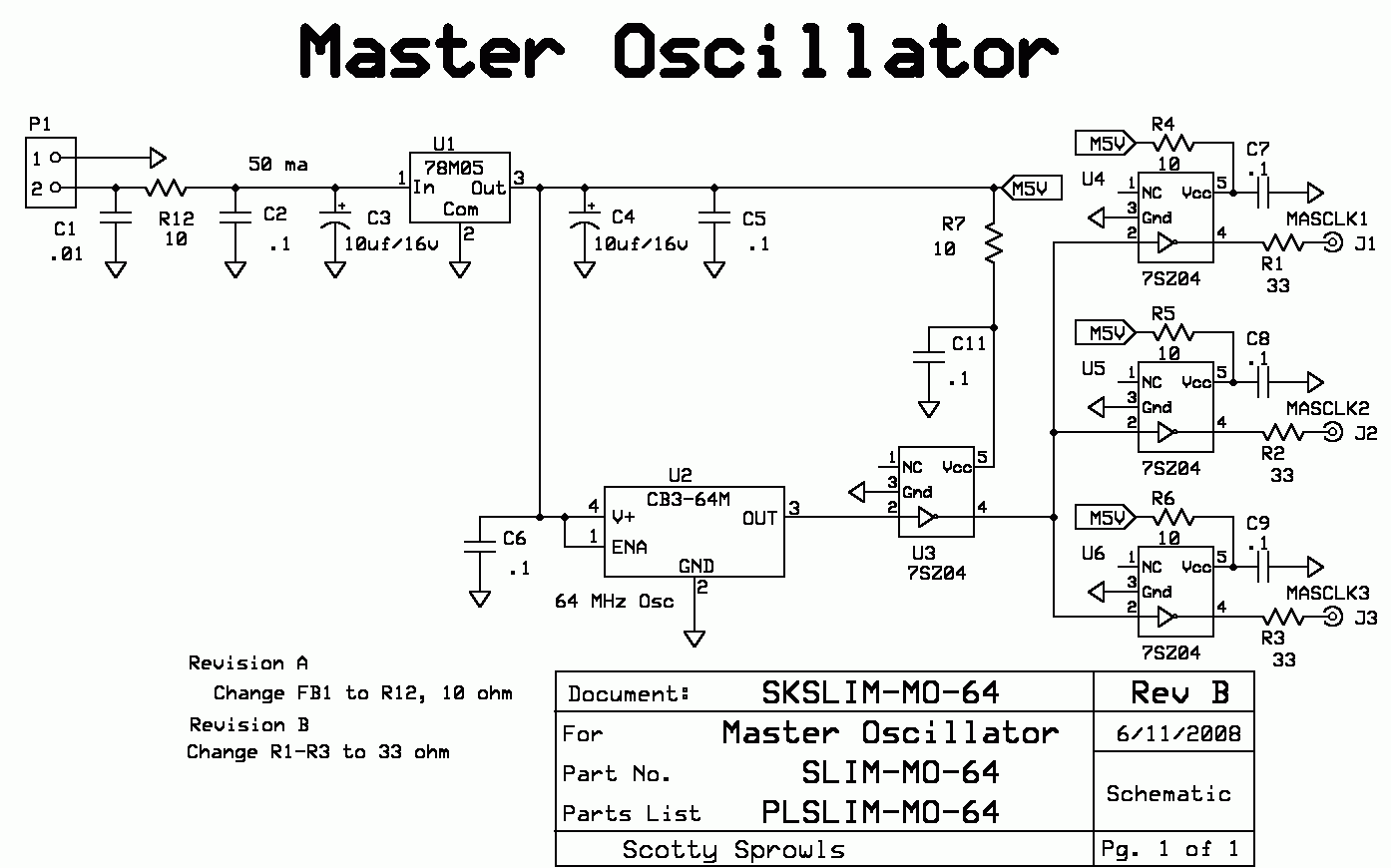
Test Procedure:
1. Verify the voltage at P1-1 is +10 volts, +/- .2 volts. The voltage at U1-1 should read about .5 volts lower than the voltage at P1-1, indicating total module current is about 50 ma.
2. Measure the +5 volts at U1-3 and U2-4. It should be +5.0 volts, +/- .1 volts.
3. Measure the voltage at U3-5. It should read about 75 mv less than U1-3.
4. Measure the voltage at U4-5, U5-5, and U6-5. Each should read about 150 mv less than U1-3 (+/- 50mv), driving a 50 ohm load. With no load, one should read about 75 mv less than U1-3(+/- 20mv).
5. Use an axial lead, 10 K ohm resistor and wrap one lead around your voltmeter probe. This will be used in the following steps to measure an average voltage. The resistor is to keep the voltmeter a high impedance load to the circuit points to be tested. A voltage reading of +2.5 volts indicates that the output has a full 5 volt peak to peak signal, although this is not an absolute verification. However, if a 0 volt or +5 volts is measured, this does indicate a failure. Measure the following points:
a. J1 and U4-4
b. J2 and U5-4
c. J3 and U6-4
d. U3-4, U4-2, U5-2, and U6-2
e. U2-3 and U3-2
DDS Module
The DDS 1 Module, SLIM-DDS-107, is the fine frequency "steering" source for PLO 1 in the MSA. The 64 MHz Master Oscillator supplies the clock signal required by the AD9850 DDS I.C. There are 2 outputs from the DDS, but only one is required for MSA operation. DDS 3 is identical to DDS 1.
This test depends on the following other modules connected and operating correctly:
Control Board, Master Oscillator Module
DDS Module Schematic, click to enlarge.
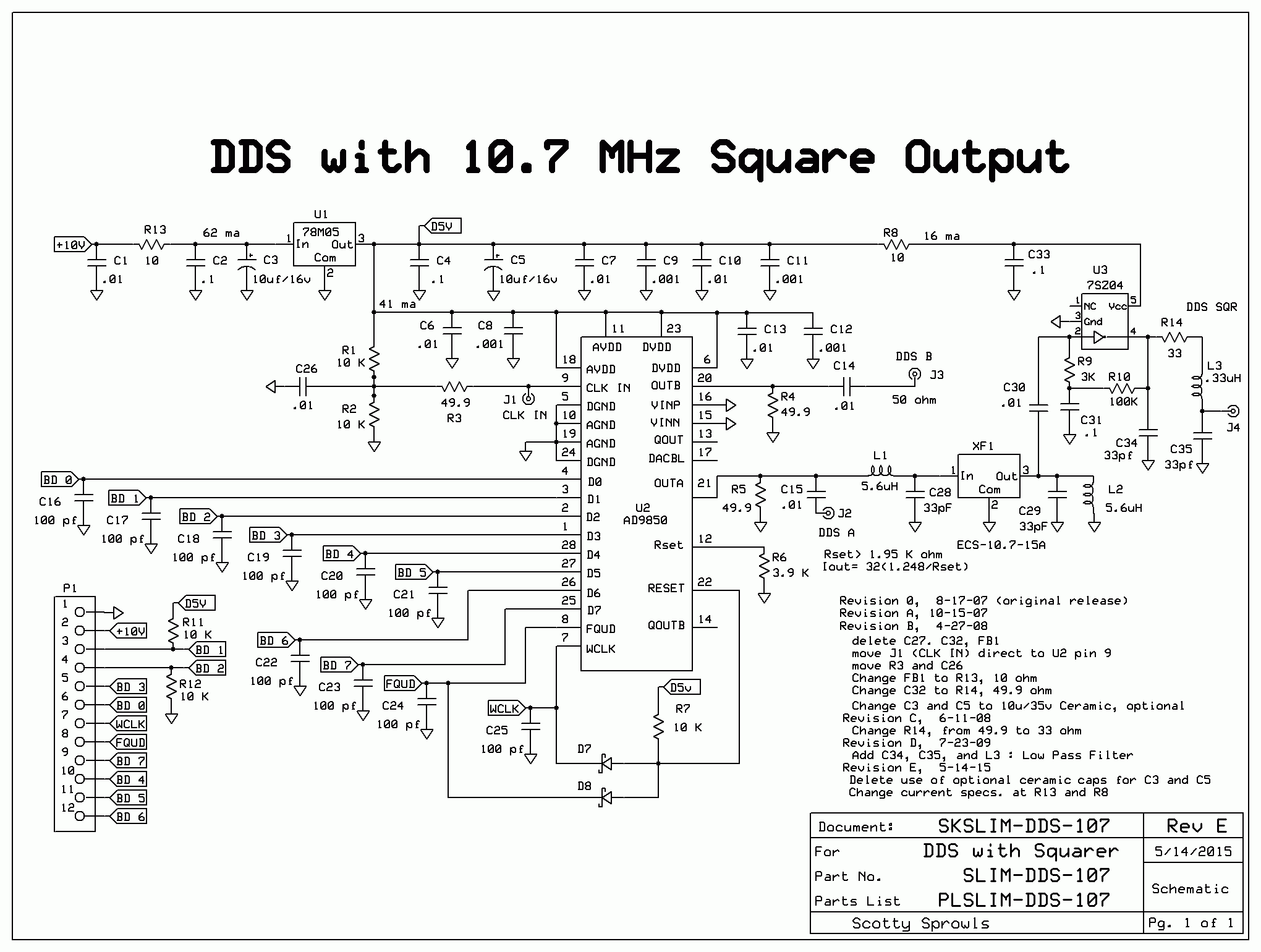
The SLIM-DDS-107 is designed and configured with a filter and squaring circuit in the DDS A path. The filter (XF1) is 10.7 MHz with a 15 KHz bandwidth. The squaring circuit of U3 will output a CMOS level, capable of driving a 50 ohm line (J4). L3/C35 comprise a low pass filter to attenuate harmonics, which have been found to affect MSA spurious. J2 is not used and should not have a connector. J3 output (the Spare) is an unfiltered output of the DDS B and will contain all harmonics and aliases of a normal DDS output. Its output power level is approximately -8 dBm.
Test Procedure:
1. Verify the MSA is sweeping.
2. Verify the voltage at P1-2 is +10 volts, +/- .2 volts. The voltage at U1-1 should be about .62 volts lower, indicating a current draw of 62 ma.
3. Measure the +5 volts at U1-3, U2-6, U2-11, U2-18, and U2-23. It should be +5.0 volts, +/- .1 volts.
4. Measure the voltage at U3-5. It should be 30 mv lower than the 5 volts measured at U1-3. This verifies current for U3 is 3 ma. If the voltage is lower (indicating higher current), U2 may not be correctly commanded to the proper frequency.
5. Measure the voltage at U3-2. It should be +2.5 volts, +/- .1 volts.
6. Measure the voltage at U2-3 and U2-4. It should be +5.0 volts, +/- .1 volts.
7. Measure the voltage at U2-1, U2-2, U2-26, U2-27 and U2-28. It should be 0 volts.
8. Measure the voltage at U2-12. It should be +1.248 volts, +/- .01 volts.
* A correct voltage here does not assure that DDS 1 is fully operational. However, an error here
does indicate a problem.
9. Repeat the previous steps for DDS 3, if incorporated into the MSA. Its voltages should be identical to DDS 1.
PLO 2 Module
The PLO 2 Module, SLIM-PLO-2, is the fixed LO frequency source for the 2nd converter in the spectrum analyzer circuit of the MSA. It is also the fixed frequency source for the Tracking Generator circuit of the MSA. This paragraph will test the basic operation of the PLO 2. Subsequent test paragraphs will verify its output power and frequency stability.
This test depends on the following other modules connected and operating correctly:
Control Board, Master Oscillator Module
This schematic is "scrunched" on the web page. Click on it to open in full view.
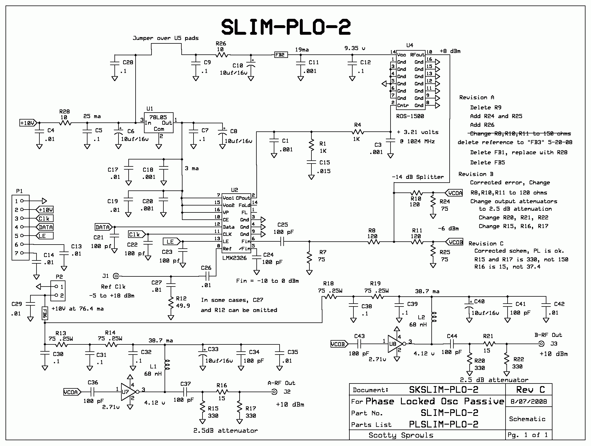
Test Procedure:
1. If the MSA is sweeping, Halt the sweep.
2. Measure and verify the voltage at these locations. Record them on your schematic.
a. P1-2 = +10 volts, +/- .2 volt.
b. U1-3 = 250 mv lower than P1-2.
c. Current = (voltage at a. - voltage at b.)/10 ohms = 25 ma., +/- 5 ma.
d. U2-7, U2-10, U2-15, U2-16 = +5.0 volts, +/-.1 volt
e. VCO supply voltage, U4-14 = +9.5 volts, +/-.2 volt (schematic voltage may not be correct)
f. VCO Current = (voltage at b. - voltage at e.)/10 ohms = 19 ma., +/- 5 ma.
g. FB6 / R13 = +10 volts, +/- .1 volt.
h. R14 / L1 = +4.12 volts, +/- .2 volt.
i. U7 Current = (voltage at g. - voltage at h.)/150 ohms = 39 ma., +/- 5 ma.
j. R19 / L2 = +4.12 volts, +/- .2 volt.
k. U8 Current = (voltage at g. - voltage at j.)/150 ohms = 39 ma., +/- 5 ma.
l. VCO Control Voltage, U4-2 = +3.2 volts, +/- .5 volt. If this voltage is +5 volts or 0 volts, it would indicate that PLO 2 is not locked.
* A high voltage suggests that U2-6 is not getting a feedback frequency from the VCO.
* A low voltage suggests that U2-8 is not getting a reference from the Master Oscillator Module.
* A command error from the Control Board may cause either high or low voltage.
PLO 1 Module
The PLO 1 Module, SLIM-PLO-1, is the variable frequency LO source for the 1st converter in the spectrum analyzer circuit of the MSA. It is also the variable frequency source for the VNA Phase circuit of the MSA. This paragraph will test the basic operation of the PLO 1. Subsequent test paragraphs will verify its output power and frequency stability. PLO 3 is identical to the PLO 1 Module.
This test depends on the following other modules connected and operating correctly:
Control Board, Master Oscillator Module, DDS 1 Module
This schematic is "scrunched" on the web page. Click on it to open in full view.
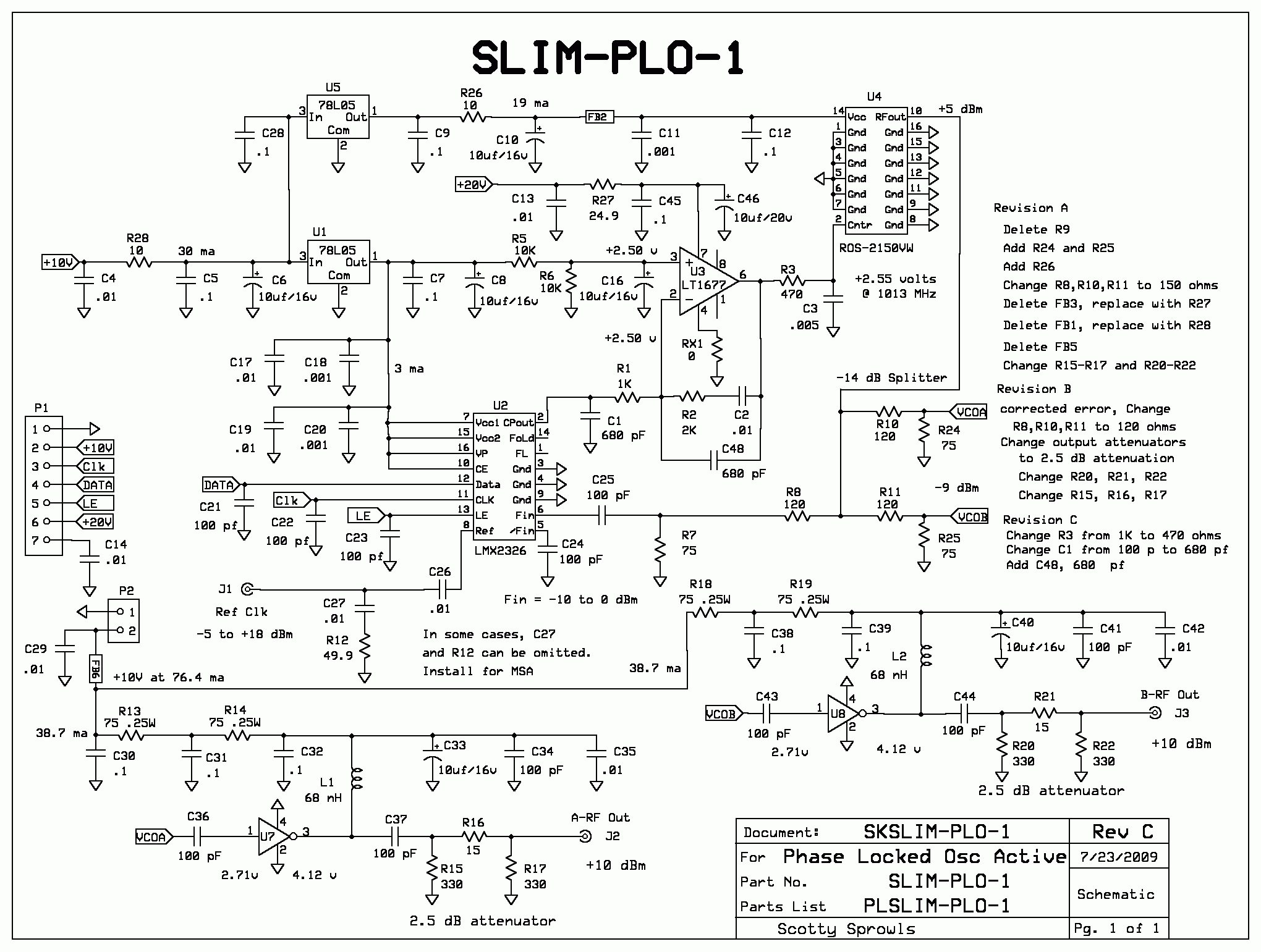
Test Procedure:
1. If the MSA is sweeping, Halt the sweep.
2. Measure and verify the voltage at these locations. Record them on your schematic.
a. P1-2 / R28 = +10 volts, +/- .2 volt.
b. U1-3 and U5-3 = +9.70 volts, +/- .2 volt.
c. Current = (voltage at a. - voltage at b.)/10 ohms = 30 ma., +/- 5 ma.
d. U2-7, U2-10, U2-15, U2-16 = +5.0 volts, +/-.1 volt
e. U5-1 = +5.0 volts, +/-.1 volt
f. VCO supply voltage, U4-14 = +4.8 volts, +/-.1 volt
g. VCO Current = (voltage at e. - voltage at f.)/10 ohms = 19 ma., +/- 5 ma.
h. 20 volt supply, P1-6 / R27 = +19.0 volts, +/-.2 volt
i. U3 supply voltage, U3-7 = +18.94 volts, +/-.2 volt. If you have an optional oscilloscope, the peak to peak ripple at U3-7 should be less than 2 millivolts. The ripple frequency is between 8 KHz and 15 KHz.
j. U3 Current = (voltage at h. - voltage at i.)/24.9 ohms = 3 ma., +/- 1 ma.
k. Bias voltage, U3-3 = +2.5 volts, +/-.2 volt.
l. Loop Balance voltage, U3-2 = exactly the same as U3-3. Any error may indicate an unlocked condition. Your DVM must be high impedance (>1 Meg Ohms) for correct results.
m. VCO Control Voltage at U4-2 = +2.55 volts, +/- .5 volt. If this voltage is +19 volts or 0 volts, it would indicate that the PLL is definitely, not locked.
* A high voltage suggests that U2-6 is not getting a feedback frequency from the VCO.
* A low voltage suggests that U2-8 is not getting a steering frequency from the DDS 1.
* A command error from the Control Board may cause either high or low voltage.
n. FB6 / R13 = +10 volts, +/- .1 volt.
o. R14 / L1 = +4.12 volts, +/- .2 volt.
p. U7 Current = (voltage at g. - voltage at h.)/150 ohms = 39 ma., +/- 5 ma.
q. R19 / L2 = +4.12 volts, +/- .2 volt.
r. U8 Current = (voltage at g. - voltage at j.)/150 ohms = 39 ma., +/- 5 ma.
PLO 3 Module
The PLO 3 Module is the variable frequency LO source for the converter in the Tracking Generator circuit of the MSA. It is also the variable frequency source for the VNA Phase circuit of the MSA. The PLO 3 Module is identical to the PLO 1 Module and share a common part number, SLIM-PLO-1. PLO 3 is tested the same way as PLO 1. Use the procedure and expected results in the previous paragraph. The results are identical, with one exception. Since PLO 3 is commanded to 1034 MHz, the VCO Control Voltage at U4-2 will be +1.5 volts, +/- .5 volt.
Test Procedure:
1. If the MSA is sweeping, Halt the sweep.
2. Measure and verify the voltage at these locations. Record them on your schematic.
a. P1-2 / R28 = +10 volts, +/- .2 volt.
b. U1-3 and U5-3 = +9.70 volts, +/- .2 volt.
c. Current = (voltage at a. - voltage at b.)/10 ohms = 30 ma., +/- 5 ma.
d. U2-7, U2-10, U2-15, U2-16 = +5.0 volts, +/-.1 volt
e. U5-1 = +5.0 volts, +/-.1 volt
f. VCO supply voltage, U4-14 = +4.8 volts, +/-.1 volt
g. VCO Current = (voltage at e. - voltage at f.)/10 ohms = 19 ma., +/- 5 ma.
h. 20 volt supply, P1-6 / R27 = +19.0 volts, +/-.2 volt
i. U3 supply voltage, U3-7 = +18.94 volts, +/-.2 volt. If you have an optional oscilloscope, the peak to peak ripple at U3-7 should be less than 2 millivolts. The ripple frequency is between 8 KHz and 15 KHz.
j. U3 Current = (voltage at h. - voltage at i.)/24.9 ohms = 3 ma., +/- 1 ma.
k. Bias voltage, U3-3 = +2.5 volts, +/-.2 volt.
l. Loop Balance voltage, U3-2 = exactly the same as U3-3. Any error may indicate an unlocked condition. Your DVM must be high impedance (>1 Meg Ohms) for correct results.
m. VCO Control Voltage at U4-2 = +2.90 volts, +/- .5 volt. If this voltage is +19 volts or 0 volts, it would indicate that the PLL is definitely, not locked. Notice the voltage is about .17 volts higher than what was measured during the PLO 1 test. This is due to the difference in frequencies.
n. FB6 / R13 = +10 volts, +/- .1 volt.
o. R14 / L1 = +4.12 volts, +/- .2 volt.
p. U7 Current = (voltage at g. - voltage at h.)/150 ohms = 39 ma., +/- 5 ma.
q. R19 / L2 = +4.12 volts, +/- .2 volt.
r. U8 Current = (voltage at g. - voltage at j.)/150 ohms = 39 ma., +/- 5 ma.
Phase Detector Module
The main purpose of this paragraph is to test the operation of the Phase Detector Module, SLIM-PDM. Basic MSA users may skip this paragraph.
This test depends on all other modules connected and operating correctly:
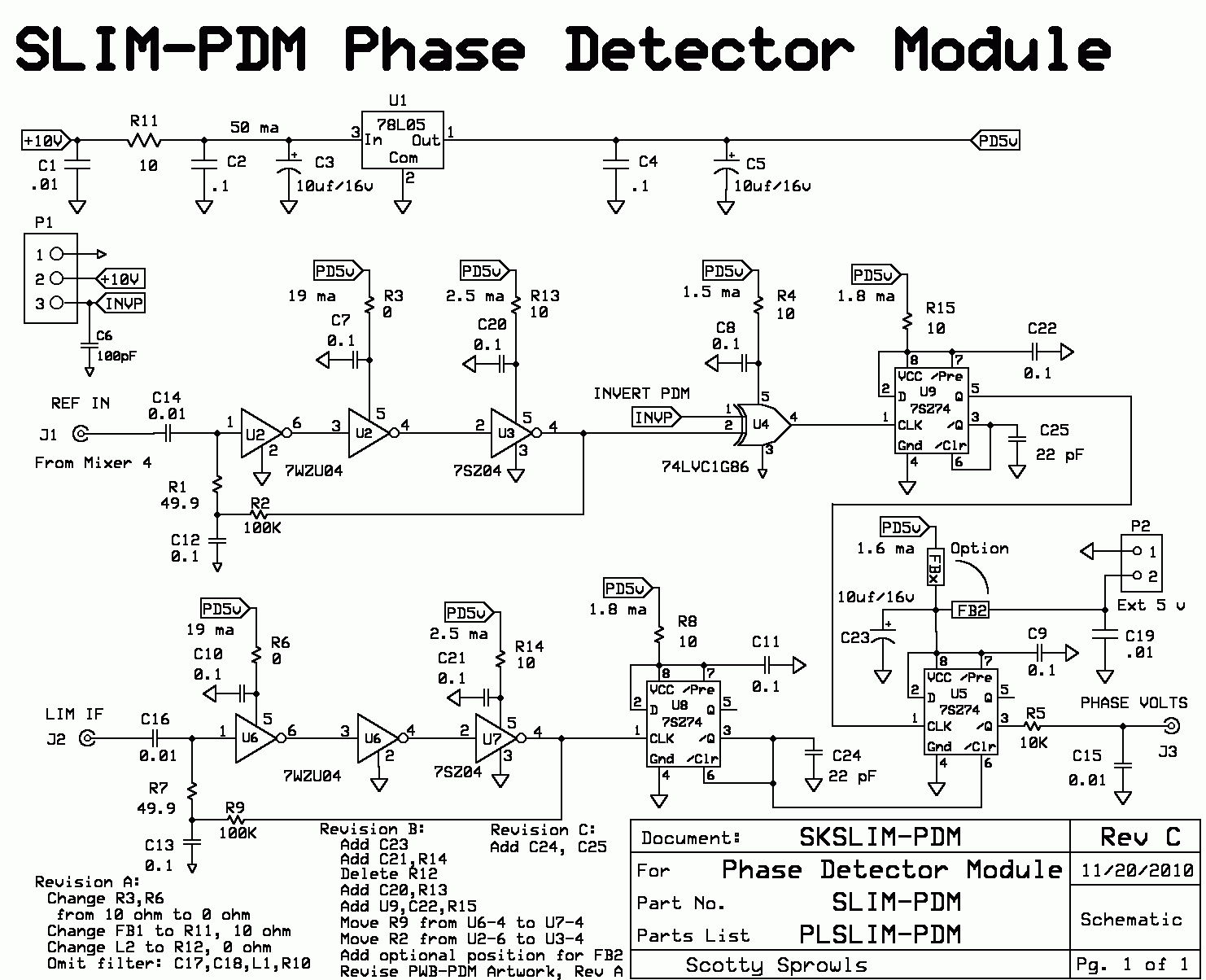
Test Procedure:
1. Run the MSA Program. The MSA Main Graph will open and sweep with the MSA in the Spectrum Analyzer mode.
2. Halt the Sweep. Connect a coaxial test cable from the Tracking Generator output to the MSA input.
3. Change Mode to VNA-Transmission Mode.
4. Halt the Sweep
5. Open the Sweep Parameters Window and change:
a. Center Frequency to 300 (MHz)
b. Span to 100 (MHz)
c. Wait to 50
6. Click "OK" to close Sweep Parameters Window.
7. Click "Restart".
8. The Magnitude trace should be about -11 dBm, +/- 2 dB.
9. Measure and verify the voltage at these locations. Record them on your schematic.
a. P1-2 / R11 = +10 volts, +/- .2 volt.
b. U1-3 = +9.50 volts, +/- .2 volt.
c. Current = (voltage at a. - voltage at b.)/10 ohms = 50 ma., +/- 5 ma.
d. U5-2, U5-7, U5-8, U2-5, U6-5 = +5.0 volts, +/-.1 volt
e. U3-5, U7-5 = 25 mv less that measured at step d, +/- 5 mv.
f. U4-5 = 15 mv less that measured at step d, +/- 2 mv.
g. U9-2, U9-7, U9-8 = 18 mv less that measured at step d, +/- 2 mv.
h. U8-2, U8-7, U8-8 = 18 mv less that measured at step d, +/- 2 mv.
i. U2-1, U6-1 = +2.50 volts, +/- .1 volt.
10. If you have an optional oscilloscope with at least a 20 MHz bandwidth, measure:
a. J1 = 200 mv peak to peak, +/- 50 mv
b. J2 = 40 mv peak to peak, +/- 10 mv
IF Amplifier Module
Updated Oct. 10, 2010 Added more information to Master Oscillator Voltage Tests
Updated Dec. 25, 2012 Changed Cavity Filter sweep test (available with MSA Software version 116)
You can link to a specific SLIM's web page by clicking on the module's paragraph header. Here are other links supporting the MSA :
Main Page for MSA Main page for the MSA.
Construction page for the SLIM MSA.
The purpose of this page is to help the MSA builder test a fully integrated MSA using minimum test equipment. I have written this page with a VOM (Volt-Ohm-Meter) as the primary piece of test equipment. In some cases of troubleshooting, higher level test equipment will be required, but I will try to keep it as simple as possible.
There are three reasons to use the procedures on this page.
1. Your MSA is functioning correctly and you just want to verify operations to get that "warm fuzzy feeling". For this, use the Verification Procedure.
2. Your MSA is not functioning within its specified capabilites. For this, use the Verification Procedure.
3. Your MSA is not operating at all, a "Hard Failure". For this, use the Troubleshooting Guide.
For any reason, this page consists of multiple tests that will verify the operation of each SLIM within a completed MSA/TG/VNA. This page is composed of four sections.
I. Troubleshooting Guide
A step-by-step procedure to help find a "Hard Failure" in the MSA. A "Hard Failure" is when the MSA is not operating at all. If the MSA is not performing to its specifications, it is considered a "Soft Failure" and it is more appropriate to follow the Verification Procedure to fix the problem.
II. Verification Procedure
Step-by-step procedures to verify the full functionality of the MSA. If a failure is encountered in these steps, it will refer you to perform a separate test in one, or both, of the next two sections.
III. SLIM Voltage Tests
Step-by-step procedures to measure and verify operating voltages within each SLIM of the MSA.
IV. Dynamic Signal Tests
Step-by-step procedures to allow the tester to minipulate signals that verify operation of the SLIMs.
This page is most relevant for an MSA using the "Direct Coaxial Connection" method of attaching RF cables, or for a connectorized MSA when the builder wishes to test or troubleshoot with minimal RF cable disconnections. For either, it is assumed that the MSA is completely integrated with all SLIMs and the wiring harness is completely inter-connected. Disregard testing of modules not present. If your MSA is partially integrated and is using RF connectors, refer to the page, Test-As-You-Build.
Items Required for Testing the Integrated MSA:
1. Completely integrated Basic MSA, MSA with Tracking Generator, or MSA/VNA
2. External DC power supply or wall wart rated at a nominal +13.6v, 1000 ma.
3. Computer with LPT port (parallel printer port) or Cypress USB Board interface.
4. Volt-Ohm Meter (VOM, Digital or Analog). All voltage measurements are DC unless noted.
5. Optional Oscilloscope, but may be necessary for troubleshooting a faulty module.
6. Software: MSA Program as spectrumanalyzer.exe (executable) or spectrumanalyzer.bas (Liberty Basic)
Set-Up, common for all testing on this page:
1. It is assumed that the MSA Software has been downloaded from the MSA Web Site and has been initialized. If not, go to the Web Page: Initial Set Up and Calibration. Follow the instructions for inital running of the MSA Software. You can run the ".bas" application with Liberty Basic as the main program, or the ".exe" application without Liberty Basic.
2. Apply power (+13.6 v nominal) to the Control Board. The Control Board supplies the necessary voltages to the other SLIMs in the MSA.
3. Connect the Control Board LPT connector to the Parallel Port of the Computer or the USB Interface.
4. Most of the tests will ask you to "Run the MSA Program". The MSA Main Graph will open and sweep with the MSA in the Spectrum Analyzer mode, 1G Band. An operational MSA will sweep with the Magnitude trace indicating the Final Crystal Filter response centered at (or near) "0 MHz".
I. Troubleshooting Guide for the MSA
Hard Failures for Basic MSA
A "Hard Failure" is when the MSA is not operating at all. The Magnitude trace will be flat, with no remarkable pattern, and will be at one of three levels: 0 dBm, -120 dBm, or in between 0 and -120 (probably about -100 dBm).
Set-Up for Troubleshooting a Hard Failure
1. Run the MSA Program. The MSA Main Graph will open and sweep with the MSA in the Spectrum Analyzer mode, 1 G Band, Path 1.
2. If entering the Troubleshooting after the initial "turn-on" of a newly completed MSA, Path 1 has default calibration values: 0 bits = -120 dBm, 32767 bits = 0dBm. This is fine.
3. Video Filter to Wide.
4. If not previously done, Halt the sweep, open the Magnitude Scale Window (Axis Y2 Window), and change the Top Ref to 0 and the Bot Ref to -120. Click "OK", the Window will close.
5. Open Variables Window (under Menu, Options) to display Magdata (dBm) and magpower (bits).
6. Click "Restart".
If the Magnitude (magpower) is a flat trace at -120 dBm or at 0 dBm (and Magdata = 65534 or 0), there is a high probability that the failure can be attributed to one of the following (in order of testing): Computer (addressing), Control Board, A to D Converter Module, and Log Detector Module (or their interconnecting wires or cables). If the Magnitude is a flat trace (with a little noise) somewhere between -120 dBm and 0 dBm, the failure will more likely be attributed to one of the other modules (or their interconnecting wires or cables). Testing will continue in the following order: PLO 2, DDS 1, PLO 1, Master Oscillator, I.F. Amplifier, Final Crystal Filter, and Coaxial Cavity Filter.
Procedure for Troubleshooting a Hard Failure
Test your MSA in the following order. Once a problem is determined and fixed, the Magnitude trace should revert to a normal level. If it doesn't, continue with the procedure until it does.
Computer (hardware)
Verify your computer Status lines are pulled up via computer or Control Board. A failure here will indicate that the computer can not "listen" to the Control Board.
a. Measure the voltage at Control Board, LPT, pin 12 and pin 13. Must be greater than + 2.0 volts.
If it is not, you must add the pull-up resistors, R9 through R12 on the Control Board or on the Cypress USB board.
Computer (addressing)
Verify "Port" signals are active, to assure Computer is "talking".
a. Measure the "Port" signal on the Control Board, using a voltmeter (Contol Board ground to LPT-2).
This is an active TTL clock signal and measured voltages will vary. However,
* a DC voltage reading should be between +.3 and +2.0 volts. If it is, continue at step 2.b.
* A 0 volt reading indicates a problem with the computer or LPT cable,
* remove the LPT cable from the computer and repeat the measurement directly on
the Parallel Port connector (pin 2 is "Port", pin 25 is ground). If good here, but not on the
Contol board, the LPT cable is bad. If not good here,
* the Port Address is incorrect for your Parallel Port interface.
* Determine correct Parallel Port Address. Install it in the Hardware Configuration Manager.
Control Board
Verify "Control" and "Port" signals are active, to assure Control Board is "listening".
a. Measure the "Port" signal at Control Board, P1-2 (common CLK to other modules)
* This is an active CMOS clock signal and measured voltages will vary, however
* a DC voltage reading should be between +.3 and +2.0 volts
* if it is, the computer and Control Board are operating.
* a 0 volt reading indicates a problem with the Control Board,
* go to the section, SLIM Voltage Tests and perform the paragraph, Control Board.
A to D Converter Module
This is the only portion of the MSA that "talks" to the computer.
a. Go to section, SLIM Voltage Tests, and perform the paragraph, A to D Module.
b. Go to section, Dynamic Signal Tests, and perform the paragraph, A to D Converter Signal Test.
Log Detector Module
a. Go to section, SLIM Voltage Tests, and perform the paragraph, Log Detector Module.
b. Go to section, Dynamic Signal Tests, and perform the paragraph, Log Detector Signal Test.
IF Amplifier Module
a. Go to section, SLIM Voltage Tests, and perform the paragraph, I.F. Amplifier Module.
b. Go to section, Dynamic Signal Tests, and perform the paragraph, I.F. Amplifier Noise Test.
Master Oscillator Module
a. Go to section, SLIM Voltage Tests, and perform the paragraph, Log Detector Module.
b. Go to section, Dynamic Signal Tests, and perform the paragraph, Master Oscillator Signal Test.
PLO 2 Module
a. Go to section, SLIM Voltage Tests, and perform the paragraph, PLO 2 Module.
DDS 1 Module
a. Go to section, SLIM Voltage Tests, and perform the paragraph, DDS Module.
b. Go to section, Dynamic Signal Tests, and perform the paragraph, DDS Command Test, and
c. go to section, Dynamic Signal Tests, and perform the paragraph, DDS 1 Signal Test.
PLO 1 Module
a. Go to section, SLIM Voltage Tests, and perform the paragraph, PLO 1 Module.
Final Crystal Filter
a. Go to section, Dynamic Signal Tests, and perform the paragraph, Final Crystal Filter Test.
Coaxial Cavity Filter
a. Go to section, Dynamic Signal Tests, and perform the paragraph, Coaxial Cavity Filter Test.
DDS 3 Module (if installed)
a. Go to section, SLIM Voltage Tests, and perform the paragraph, DDS Module.
b. Go to section, Dynamic Signal Tests, and perform the paragraph, DDS Command Test, and
c. go to section, Dynamic Signal Tests, and perform the paragraph, DDS 3 Signal Test
PLO 3 Module (if installed)
a. Go to section, SLIM Voltage Tests, and perform the paragraph, PLO 3 Module.
Phase Detector Module (if installed)
a. Go to section, SLIM Voltage Tests, and perform the paragraph, Phase Detector Module.
Soft Failures
A "Soft Failure" is when the MSA is not performing to specification. Use the Verification Procedure.
II. Verification Procedure
Test Sequence for Verification:
Voltage Tests
Go to the section, SLIM Voltage Tests and, for the:
1. Control Board, perform the paragraph, Control Board.
2. Analog to Digital Converter, perform the paragraph, A to D Module.
3. Log Detector, perform the paragraph, Log Detector Module.
4. Master Oscillator, perform the paragraph, Master Oscillator.
5. I.F. Amplifier, perform the paragraph, I.F. Amplifier Module.
6. DDS 1, perform the paragraph, DDS Module.
7. PLO 2, perform the paragraph, PLO 2 Module.
8. PLO 1, perform the paragraph, PLO 1 Module.
9. DDS 3, perform the paragraph, DDS Module, (if installed)
10. PLO 3, perform the paragraph, PLO 3 Module, (if installed)
11. Phase Detector, perform the paragraph, Phase Detector Module, (if installed)
Performance Tests
12. Perform the "Zero" Frequency Sweep Test. Compare the data of your MSA to the data given in the test procedure to determine the performance of your MSA.
a. During this test, determine if the L.O. power at Mixer 2 is adequite:
* In Mixer 2, short over the attenuation resistor, R5. This increases the LO power by 1.3 dB.
* If the final Magnitude measurement increases by more than .5 dB, the mixer is "starved" and
steps should be taken to increase the RF power at Mixer 2, J1.
13. Perform the DDS 1 Generator Test. This is a good indication of the measurement accuracy of the Spectrum Analyzer at 10.7 MHz.
a. During this test, determine if the L.O. power at Mixer 1 is adequite:
* In Mixer 1, short over the attenuation resistor, R5. This increases the LO power by 1.3 dB.
* If the final Magnitude measurement increases by more than .5 dB, the mixer is "starved" and
steps should be taken to increase the RF power at Mixer 1, J1.
14. Perform the I.F. Amplifier Signal Test.
15. If your Final Crystal Filter is removable, perform the Optional Coaxial Cavity Filter Test. This test will indicate the general "health" of the Coaxial Cavity Filter.
16. For the MSA with Tracking Generator, perform the MSA Frequency Range Test.
Block Diagram for the MSA/VNA
The block diagram shows typical power levels, but not all due to the builder's preference of internal attenuators. Listed here are measured values from the Verification SLIM MSA:
a. Gains = +40 dB (I.F. Amplifier)
b. Losses:
* Mixer 1 conversion loss = -6.5 dB, with - 4.7 dB of attenuator at J2 = -11.2 dB
* L to R port isolation of Mixer 1 = -35 dB, +/- 10.0 dB
* Coaxial Cavity Filter insertion loss = -5.3 dB
* Mixer 2 conversion loss = -6.5 dB
* Path 1 Resolution Filter insertion loss = -4 dB, +/- 1.0 dB
* Mixer 3 conversion loss = -6.5 dB, with - 14 dB of attenuator at J3 = -20.5 dB
* Mixer 4 conversion loss = -6.5 dB, with - 14 dB of attenuator at J3 = -20.5 dB
c. Total gain of Spectrum Analyzer chain, from MSA input to Log Detector input = +13.0 dB
d. Tracking Generator output power = -10.5 dBm, at 100 MHz.
Wiring Diagram for the MSA/VNA
III. SLIM Voltage Tests
The following Test Paragraphs are voltage measurements within each SLIM. Voltages that are out of tolerance will usually indicate a problem within that module. Click the paragraph header to link to the SLIM's web page.
Control Board
The Control Board contains all of the interfacing between the computer and the individual SLIM modules. It also contains the voltage regulation needed for the other modules. The Control Board requires +12 volts to +18 volts DC at 1 amp of peak current. For full MSA operation, the Control Board will use and pass on about 750 ma.
This is the latest schematic of the MSA Control Board. If your Control Board is an earlier version, you will want to test if pull-up resistors are required for your computer. Most home computers do not need them.
Test Procedure:
1. Measure the voltage at these locations, as indicated in the schematic:
a. SELECT and PE. The voltage should read a minimum of 2.0 volts, maximum of 5.0 volts. If you read less than the minimum voltage, remove power, disconnect from the computer and add the pull-up resistors, R9-R12.
b. WAIT and ACK. The voltage should read either a "zero" or "one". A "zero" is 0 volts +.2v. A "one" should read a minimum of 2.0 volts, a maximum of 5.0 volts. If you read less than the minimum voltage, remove power, disconnect from the computer and add the pull-up resistors, R9-R12.
2. Measure the input voltage to the Control Board at U5-1. Range: +12.0 v to +18 v.
3. Measure the output of the +10 volt regulator, U5-3. It should be +10.0 volts, +/- 0.2 volts.
4. Measure the output of the +5 volt regulator, U6-1. It should be +5.0 volts, +/- 0.2 volts.
5. LED 1 should be lit.
6. Measure the output of the +20 volt multiplier at P23-2 and P24-2. It should be +18.94 volts +/- .3 volts.
7. If you have an oscilloscope, measure the peak to peak ripple at P23-2 or P24-2. It should be less than 20.0 millivolts. When the MSA is completed, excessive ripple will be seen as side bands on every signal when in the Spectrum Analyzer Mode. A cure is too add more capacitance at C20, C21, C23, C24, and C25.
8. If C15 is installed, measure the -10 volt multiplier at P23-3 and P24-3. It should be -10.0 volts, +/- 0.3 volts. The -10 volts is not used in the SLIM MSA, but can be utilized for external experiments requiring current less than 20 ma.
AtoD Module
The following is written for the SLIM-ADC-16. The procedure is the same when using the SLIM-ADC-12.
This test depends on the following other modules connected and operating correctly: Control Board
This schematic shows the U1 regulator installed. This is the case for the Basic MSA. For the VNA, it may be ommitted and there must be a jumper wire from the pwb pads of U1-3 to U1-1. Power is supplied from the PDM module's J2-1 and J2-2 to the AtoD module's J1-1 and J1-2. The name "+10v" should be changed to "+5v". Make certain that the PDM module has its ferrite jumpers installed (FBx and FB2).
Test Procedure
1. For the Basic MSA, verify the voltage at U1-3 is +10 volts, +/- .2 volts. For the VNA (no U1) verify the voltage is +5.0 volts, +/- .1 volts.
2. Measure the +5 volts at U1-1, U2-1, U2-2, U2-9, U2-10. It should be +5.0 volts, +/- .1 volts.
3. Measure the +5 volts at U3-1, U3-2, U3-9, U3-10 (if U3 if installed). It should be +5.0 volts, +/- .1 volts. U3 may not be installed for the Basic MSA version.
4. Halt the sweep.
5. Measure the voltage at U2-3. This is the Magnitude output voltage of the Log Detector Module. Its voltage level depends entirely upon the amount of RF power applied to J1 of the Log Detector Module. The voltage should read between +.3 volts and +2.5 volts. A 0 volts reading might indicate a short or low resistance path to ground. A much higher voltage might indicate a short or low resistance path to +5v. If so, inspect for shorts or cleanliness.
6. The voltage at U3-3, if installed, is the Phase output voltage of the Phase Detector Module. Its voltage level is relevant only during a normal VNA set-up condition. However, a 0 volts reading might indicate a short or low resistance path to ground. A +5 volts reading might indicate a short or low resistance path to +5v. If so, inspect for shorts or cleanliness. This voltage will be more critically tested in a later paragraph.
Log Detector Module
The Log Detector Module, SLIM-LD-8306, converts RF power to voltage in a logarithmic function. The bandwidth of the module is 2 MHz to 160 MHz, although the input will be 10.7 MHz in the MSA.
The J2 output is the Magnitude voltage output which goes to the AtoD Module. Its J1 input dynamic range is from approximately -90 dBm to +10 dBm, although this range might be extended. Its J2 output voltage over this range is approximately .35 volts to 2.35 volts.
The J3 output is an RF Limited output of the input frequency. It supplies the Signal Input to the PDM Module (VNA only). The module does not require any direct commands from the computer, and it can be partially tested with only a voltmeter.
This test depends on the following other modules connected and operating correctly:
Control Board, A to D Module
*Note: You may modify the Log Detector Module for AC coupled input by cutting the trace between J1 and the input to transformer T1 and adding a series capacitor (.1 ufd). You may leave the capacitor in place without affecting the characteristics of the Log Detector.
Test Procedure:
1. Verify the voltage at U1-3 is +10 volts, +/- .2 volts.
2. Measure the +5 volts at U1-1. It should be +5.0 volts, +/- .1 volts.
3. Measure the +5 volts at U2-2 and U2-8. It should be about 92 millivolts less than the voltage measured at U1-1.
4. Measure the +5 volts at U2-15. It should be about 64 millivolts less than the voltage measured at U1-1.
5. Measure the voltage at U2-9. It should be +.41 volts, +/- .05 volts if R6 is 390 ohms.
6. Measure the voltage at U2-12 and U2-13. They should be about 25 millivolts less than the voltage measured at U1-1. This is the Limited I.F. output and can be observed with an optional 20 MHz o'scope. With no input signal to the Log Detector, either pin should be about 60 mv peak to peak noise. If a signal is input to the Log Detector, either pin should be about 60 mv peak to peak square wave. If the PDM is connected to J3 of the Log Detector Module, the peak to peak value at U2-12 will be one half that, or 30 mv pp.
7. Measure the voltage at U2-16 and J2. This is the Magnitude output voltage of the Log Detector Module. Its voltage level depends entirely upon the amount of RF power applied to J1 of the Log Detector Module. The voltage should read between +.3 volts and +2.5 volts. A 0 volts reading might indicate a short or low resistance path to ground. A much higher voltage might indicate a short or low resistance path to +5v. If so, inspect for shorts or cleanliness.
Master Oscillator Module
The Master Oscillator Module, SLIM-MO-64, incorporates a 64 MHz crystal oscillator and 3 buffers for distribution to the other SLIMs. This section will test the MO for basic operation but not for frequency accuracy.
This test depends on the following other modules connected and operating correctly: Control Board
Test Procedure:
1. Verify the voltage at P1-1 is +10 volts, +/- .2 volts. The voltage at U1-1 should read about .5 volts lower than the voltage at P1-1, indicating total module current is about 50 ma.
2. Measure the +5 volts at U1-3 and U2-4. It should be +5.0 volts, +/- .1 volts.
3. Measure the voltage at U3-5. It should read about 75 mv less than U1-3.
4. Measure the voltage at U4-5, U5-5, and U6-5. Each should read about 150 mv less than U1-3 (+/- 50mv), driving a 50 ohm load. With no load, one should read about 75 mv less than U1-3(+/- 20mv).
5. Use an axial lead, 10 K ohm resistor and wrap one lead around your voltmeter probe. This will be used in the following steps to measure an average voltage. The resistor is to keep the voltmeter a high impedance load to the circuit points to be tested. A voltage reading of +2.5 volts indicates that the output has a full 5 volt peak to peak signal, although this is not an absolute verification. However, if a 0 volt or +5 volts is measured, this does indicate a failure. Measure the following points:
a. J1 and U4-4
b. J2 and U5-4
c. J3 and U6-4
d. U3-4, U4-2, U5-2, and U6-2
e. U2-3 and U3-2
DDS Module
The DDS 1 Module, SLIM-DDS-107, is the fine frequency "steering" source for PLO 1 in the MSA. The 64 MHz Master Oscillator supplies the clock signal required by the AD9850 DDS I.C. There are 2 outputs from the DDS, but only one is required for MSA operation. DDS 3 is identical to DDS 1.
This test depends on the following other modules connected and operating correctly:
Control Board, Master Oscillator Module
DDS Module Schematic, click to enlarge.
The SLIM-DDS-107 is designed and configured with a filter and squaring circuit in the DDS A path. The filter (XF1) is 10.7 MHz with a 15 KHz bandwidth. The squaring circuit of U3 will output a CMOS level, capable of driving a 50 ohm line (J4). L3/C35 comprise a low pass filter to attenuate harmonics, which have been found to affect MSA spurious. J2 is not used and should not have a connector. J3 output (the Spare) is an unfiltered output of the DDS B and will contain all harmonics and aliases of a normal DDS output. Its output power level is approximately -8 dBm.
Test Procedure:
1. Verify the MSA is sweeping.
2. Verify the voltage at P1-2 is +10 volts, +/- .2 volts. The voltage at U1-1 should be about .62 volts lower, indicating a current draw of 62 ma.
3. Measure the +5 volts at U1-3, U2-6, U2-11, U2-18, and U2-23. It should be +5.0 volts, +/- .1 volts.
4. Measure the voltage at U3-5. It should be 30 mv lower than the 5 volts measured at U1-3. This verifies current for U3 is 3 ma. If the voltage is lower (indicating higher current), U2 may not be correctly commanded to the proper frequency.
5. Measure the voltage at U3-2. It should be +2.5 volts, +/- .1 volts.
6. Measure the voltage at U2-3 and U2-4. It should be +5.0 volts, +/- .1 volts.
7. Measure the voltage at U2-1, U2-2, U2-26, U2-27 and U2-28. It should be 0 volts.
8. Measure the voltage at U2-12. It should be +1.248 volts, +/- .01 volts.
* A correct voltage here does not assure that DDS 1 is fully operational. However, an error here
does indicate a problem.
9. Repeat the previous steps for DDS 3, if incorporated into the MSA. Its voltages should be identical to DDS 1.
PLO 2 Module
The PLO 2 Module, SLIM-PLO-2, is the fixed LO frequency source for the 2nd converter in the spectrum analyzer circuit of the MSA. It is also the fixed frequency source for the Tracking Generator circuit of the MSA. This paragraph will test the basic operation of the PLO 2. Subsequent test paragraphs will verify its output power and frequency stability.
This test depends on the following other modules connected and operating correctly:
Control Board, Master Oscillator Module
This schematic is "scrunched" on the web page. Click on it to open in full view.
Test Procedure:
1. If the MSA is sweeping, Halt the sweep.
2. Measure and verify the voltage at these locations. Record them on your schematic.
a. P1-2 = +10 volts, +/- .2 volt.
b. U1-3 = 250 mv lower than P1-2.
c. Current = (voltage at a. - voltage at b.)/10 ohms = 25 ma., +/- 5 ma.
d. U2-7, U2-10, U2-15, U2-16 = +5.0 volts, +/-.1 volt
e. VCO supply voltage, U4-14 = +9.5 volts, +/-.2 volt (schematic voltage may not be correct)
f. VCO Current = (voltage at b. - voltage at e.)/10 ohms = 19 ma., +/- 5 ma.
g. FB6 / R13 = +10 volts, +/- .1 volt.
h. R14 / L1 = +4.12 volts, +/- .2 volt.
i. U7 Current = (voltage at g. - voltage at h.)/150 ohms = 39 ma., +/- 5 ma.
j. R19 / L2 = +4.12 volts, +/- .2 volt.
k. U8 Current = (voltage at g. - voltage at j.)/150 ohms = 39 ma., +/- 5 ma.
l. VCO Control Voltage, U4-2 = +3.2 volts, +/- .5 volt. If this voltage is +5 volts or 0 volts, it would indicate that PLO 2 is not locked.
* A high voltage suggests that U2-6 is not getting a feedback frequency from the VCO.
* A low voltage suggests that U2-8 is not getting a reference from the Master Oscillator Module.
* A command error from the Control Board may cause either high or low voltage.
PLO 1 Module
The PLO 1 Module, SLIM-PLO-1, is the variable frequency LO source for the 1st converter in the spectrum analyzer circuit of the MSA. It is also the variable frequency source for the VNA Phase circuit of the MSA. This paragraph will test the basic operation of the PLO 1. Subsequent test paragraphs will verify its output power and frequency stability. PLO 3 is identical to the PLO 1 Module.
This test depends on the following other modules connected and operating correctly:
Control Board, Master Oscillator Module, DDS 1 Module
This schematic is "scrunched" on the web page. Click on it to open in full view.
Test Procedure:
1. If the MSA is sweeping, Halt the sweep.
2. Measure and verify the voltage at these locations. Record them on your schematic.
a. P1-2 / R28 = +10 volts, +/- .2 volt.
b. U1-3 and U5-3 = +9.70 volts, +/- .2 volt.
c. Current = (voltage at a. - voltage at b.)/10 ohms = 30 ma., +/- 5 ma.
d. U2-7, U2-10, U2-15, U2-16 = +5.0 volts, +/-.1 volt
e. U5-1 = +5.0 volts, +/-.1 volt
f. VCO supply voltage, U4-14 = +4.8 volts, +/-.1 volt
g. VCO Current = (voltage at e. - voltage at f.)/10 ohms = 19 ma., +/- 5 ma.
h. 20 volt supply, P1-6 / R27 = +19.0 volts, +/-.2 volt
i. U3 supply voltage, U3-7 = +18.94 volts, +/-.2 volt. If you have an optional oscilloscope, the peak to peak ripple at U3-7 should be less than 2 millivolts. The ripple frequency is between 8 KHz and 15 KHz.
j. U3 Current = (voltage at h. - voltage at i.)/24.9 ohms = 3 ma., +/- 1 ma.
k. Bias voltage, U3-3 = +2.5 volts, +/-.2 volt.
l. Loop Balance voltage, U3-2 = exactly the same as U3-3. Any error may indicate an unlocked condition. Your DVM must be high impedance (>1 Meg Ohms) for correct results.
m. VCO Control Voltage at U4-2 = +2.55 volts, +/- .5 volt. If this voltage is +19 volts or 0 volts, it would indicate that the PLL is definitely, not locked.
* A high voltage suggests that U2-6 is not getting a feedback frequency from the VCO.
* A low voltage suggests that U2-8 is not getting a steering frequency from the DDS 1.
* A command error from the Control Board may cause either high or low voltage.
n. FB6 / R13 = +10 volts, +/- .1 volt.
o. R14 / L1 = +4.12 volts, +/- .2 volt.
p. U7 Current = (voltage at g. - voltage at h.)/150 ohms = 39 ma., +/- 5 ma.
q. R19 / L2 = +4.12 volts, +/- .2 volt.
r. U8 Current = (voltage at g. - voltage at j.)/150 ohms = 39 ma., +/- 5 ma.
PLO 3 Module
The PLO 3 Module is the variable frequency LO source for the converter in the Tracking Generator circuit of the MSA. It is also the variable frequency source for the VNA Phase circuit of the MSA. The PLO 3 Module is identical to the PLO 1 Module and share a common part number, SLIM-PLO-1. PLO 3 is tested the same way as PLO 1. Use the procedure and expected results in the previous paragraph. The results are identical, with one exception. Since PLO 3 is commanded to 1034 MHz, the VCO Control Voltage at U4-2 will be +1.5 volts, +/- .5 volt.
Test Procedure:
1. If the MSA is sweeping, Halt the sweep.
2. Measure and verify the voltage at these locations. Record them on your schematic.
a. P1-2 / R28 = +10 volts, +/- .2 volt.
b. U1-3 and U5-3 = +9.70 volts, +/- .2 volt.
c. Current = (voltage at a. - voltage at b.)/10 ohms = 30 ma., +/- 5 ma.
d. U2-7, U2-10, U2-15, U2-16 = +5.0 volts, +/-.1 volt
e. U5-1 = +5.0 volts, +/-.1 volt
f. VCO supply voltage, U4-14 = +4.8 volts, +/-.1 volt
g. VCO Current = (voltage at e. - voltage at f.)/10 ohms = 19 ma., +/- 5 ma.
h. 20 volt supply, P1-6 / R27 = +19.0 volts, +/-.2 volt
i. U3 supply voltage, U3-7 = +18.94 volts, +/-.2 volt. If you have an optional oscilloscope, the peak to peak ripple at U3-7 should be less than 2 millivolts. The ripple frequency is between 8 KHz and 15 KHz.
j. U3 Current = (voltage at h. - voltage at i.)/24.9 ohms = 3 ma., +/- 1 ma.
k. Bias voltage, U3-3 = +2.5 volts, +/-.2 volt.
l. Loop Balance voltage, U3-2 = exactly the same as U3-3. Any error may indicate an unlocked condition. Your DVM must be high impedance (>1 Meg Ohms) for correct results.
m. VCO Control Voltage at U4-2 = +2.90 volts, +/- .5 volt. If this voltage is +19 volts or 0 volts, it would indicate that the PLL is definitely, not locked. Notice the voltage is about .17 volts higher than what was measured during the PLO 1 test. This is due to the difference in frequencies.
n. FB6 / R13 = +10 volts, +/- .1 volt.
o. R14 / L1 = +4.12 volts, +/- .2 volt.
p. U7 Current = (voltage at g. - voltage at h.)/150 ohms = 39 ma., +/- 5 ma.
q. R19 / L2 = +4.12 volts, +/- .2 volt.
r. U8 Current = (voltage at g. - voltage at j.)/150 ohms = 39 ma., +/- 5 ma.
Phase Detector Module
The main purpose of this paragraph is to test the operation of the Phase Detector Module, SLIM-PDM. Basic MSA users may skip this paragraph.
This test depends on all other modules connected and operating correctly:
Test Procedure:
1. Run the MSA Program. The MSA Main Graph will open and sweep with the MSA in the Spectrum Analyzer mode.
2. Halt the Sweep. Connect a coaxial test cable from the Tracking Generator output to the MSA input.
3. Change Mode to VNA-Transmission Mode.
4. Halt the Sweep
5. Open the Sweep Parameters Window and change:
a. Center Frequency to 300 (MHz)
b. Span to 100 (MHz)
c. Wait to 50
6. Click "OK" to close Sweep Parameters Window.
7. Click "Restart".
8. The Magnitude trace should be about -11 dBm, +/- 2 dB.
9. Measure and verify the voltage at these locations. Record them on your schematic.
a. P1-2 / R11 = +10 volts, +/- .2 volt.
b. U1-3 = +9.50 volts, +/- .2 volt.
c. Current = (voltage at a. - voltage at b.)/10 ohms = 50 ma., +/- 5 ma.
d. U5-2, U5-7, U5-8, U2-5, U6-5 = +5.0 volts, +/-.1 volt
e. U3-5, U7-5 = 25 mv less that measured at step d, +/- 5 mv.
f. U4-5 = 15 mv less that measured at step d, +/- 2 mv.
g. U9-2, U9-7, U9-8 = 18 mv less that measured at step d, +/- 2 mv.
h. U8-2, U8-7, U8-8 = 18 mv less that measured at step d, +/- 2 mv.
i. U2-1, U6-1 = +2.50 volts, +/- .1 volt.
10. If you have an optional oscilloscope with at least a 20 MHz bandwidth, measure:
a. J1 = 200 mv peak to peak, +/- 50 mv
b. J2 = 40 mv peak to peak, +/- 10 mv
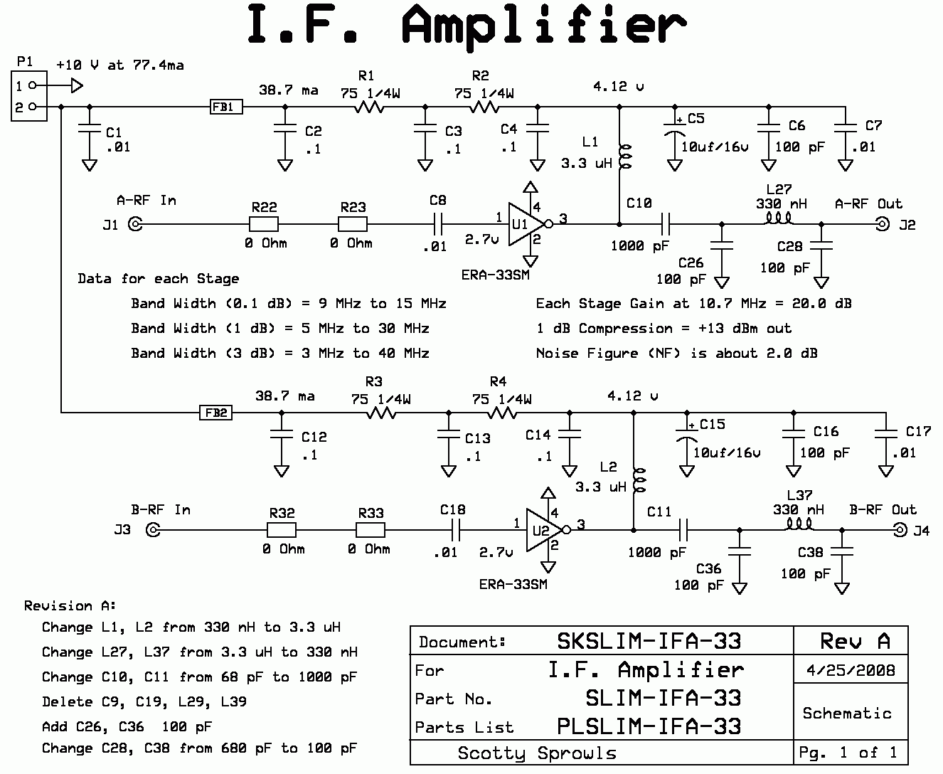
IF Amplifier Module